QUEENEMS BLOG
PCB Design & DFM Articles
Explore PCB layout, stack-ups, footprints and fabrication data. Review design decisions and manufacturing checks before releasing your files.
Need a review of your fabrication files? See the PCB DFM review service.
108 articles
PCB Guard Ring Design for Low-Leakage Input Circuits
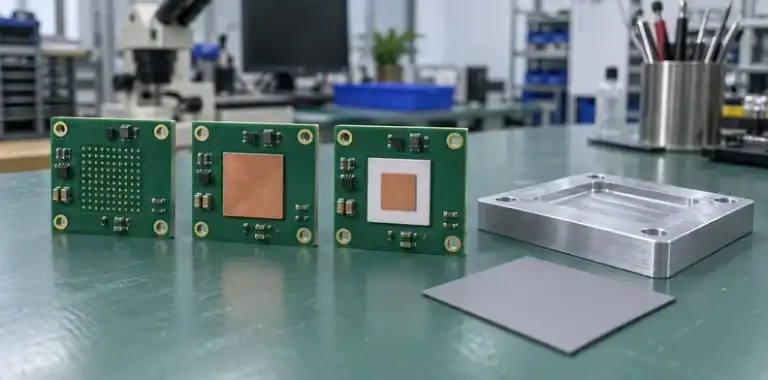
SiC MOSFET PCB Cooling: Thermal Vias, Copper Coins and AlN
Capacitive Touch PCB Design: Electrodes, Covers and Shields
RF Shielding PCB Design: Shield Cans, Clips and Land Patterns
Planar Transformer PCB Design: Winding Stack and Insulation
Semi Flex PCB Design: Thinned FR4 Bends for Fixed Installs
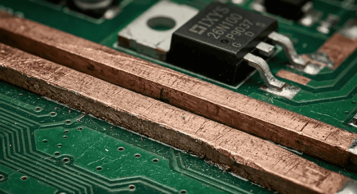
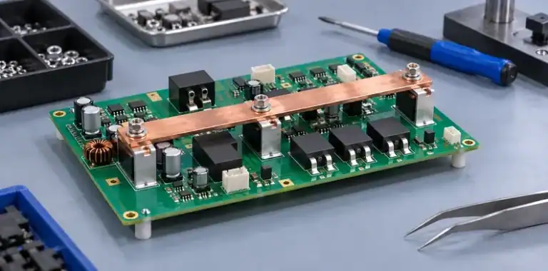
PCB Busbar Design: Joints, Copper Taps and Assembly Checks
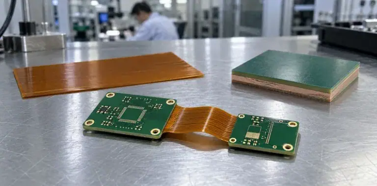
How to Avoid Hidden HDI Rigid Flex PCB Design Errors
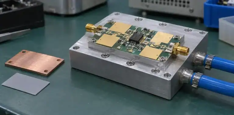
How GaN Amplifier PCB Thermal Design Changes for CW
QR Code on PCB: Avoid These Mistakes for Better Scanning
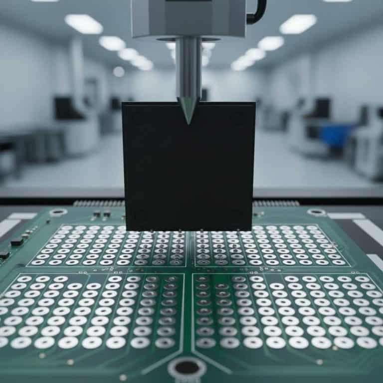
Probe Card Manufacturing: How to Specify the PCB
Single-Sided PCB or Double-Sided: How to Choose
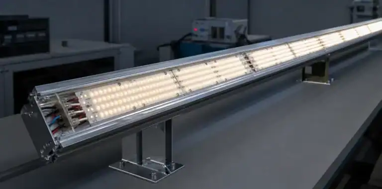
Long LED PCB Board: How to Control Dimming and Heat
Large PCB Connector Alignment Rules for Reliable Fit
Large PCB Power Distribution: A Practical Design Checklist
When a Large PCB Stiffener Solves Mechanical Load Risk
Rigid-Flex vs Large Rigid PCB for a 3D Product
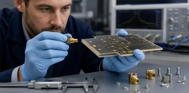
Large PCB Panelization for Better Material Use
9 Ways to Protect Large PCB Signal Integrity
One Large PCB vs Multiple Boards: What Should You Quote?
Large PCB Design Rules: How to Prevent Costly Rework
PCB Glass Weave Skew: 5 Costly Timing Mistakes
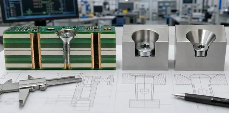
PCB Counterbore vs Countersink: 7 RFQ Rules to Know
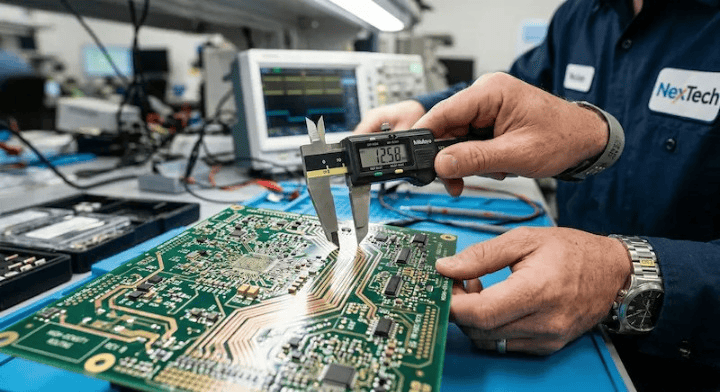
PCB Edge Connector Bevel: 5 Costly Fit Mistakes
PCB Hole Position Tolerance: 5 Costly Datum Mistakes
PCB Internal Corner Radius: 5 Costly Routing Mistakes
How to Check an AI Generated PCB Before Quote
How to Compare PCB DRC vs DFM Before Fabrication
How to Verify an AI PCB Footprint Before Quote
AI PCB Impedance Stackup: How to Avoid Fab Errors
AI PCB Gerber Review: How to Avoid CAM Holds
AI PCB Specialty Review: How to Avoid Fab Mistakes
PCB Copper Balance Mistakes That Create CAM Holds
PCB Tolerance Stack-Up Mistakes That Hurt Assembly Fit
High-Speed Backplane PCB Mistakes That Hurt Signal Integrity
7 PCB Coil Design Mistakes That Delay Fabrication
How to Choose BT PCB Thickness and Layer Count Before RFQ
Ceramic PCB Laser Diode Boards: How to Protect Heat and Alignment
RF Edge Launch PCB Thickness: Fit and Release Proof
High Frequency Hybrid PCB Stackup RFQ Evidence Buyers Need
High Speed Hybrid PCB Stackup Proof Buyers Need Before RFQ
Practical Hybrid PCB Stackup Drawing Evidence Before RFQ
Flex PCB Stiffener: How to Avoid ZIF Fit Failures
V-Score vs Tab Routing Buyers Can Put in an RFQ
High Voltage PCB Design Buyers Can Put in an RFQ
How to Choose PCB Thickness: Standard Sizes and Fit
What processed Gerber approval catches in risky CAM edits
What PCB stackup approval risks cost buyers the most
How to Specify PCB Countersink Holes Without Costly Fit Errors
Peelable Solder Mask: How to Prevent Removal Damage
Copper Thieving on PCBs: Requirements, Clearances and Drawing Notes
PCB Teardrops: How to Approve a CAM Change
How to Set PCB Outline Tolerance Without Costly Fit Errors
How to Prevent Solder Mask Bridge Failures Before PCB Release
PCB Silkscreen: How to Keep Markings Readable After Assembly
What a PCB DFM Review Before PO Must Close First
What PCB Plated Slot Details Belong in the RFQ?
What PCB edge plating requirements: 5 Buyer Risks
PCB Castellated Holes Requirements: Design Rules, Plating and Footprint
How to Review PCB Press-Fit Hole Tolerance
PCB Tooling Holes Requirements: Size, Placement and Plating
PCB Solder Mask Opening Requirements: NSMD vs SMD, Expansion and Dams
PCB Copper-to-Edge Clearance Requirements: Routed, V-Score and Plated Edges
How to Control a PCB Production Release Package
How to Review PCB Panel Drawing Approval
How to Close PCB CAM Questions Before Production
How to Design an HDI PCB for PCIe 5.0 & DDR5
HDI Any-Layer ELIC: When Does Your Board Need It?
HDI with Embedded Components: Design and RFQ Checks
IPC-2226 HDI Types: Type I vs Type II vs Type III
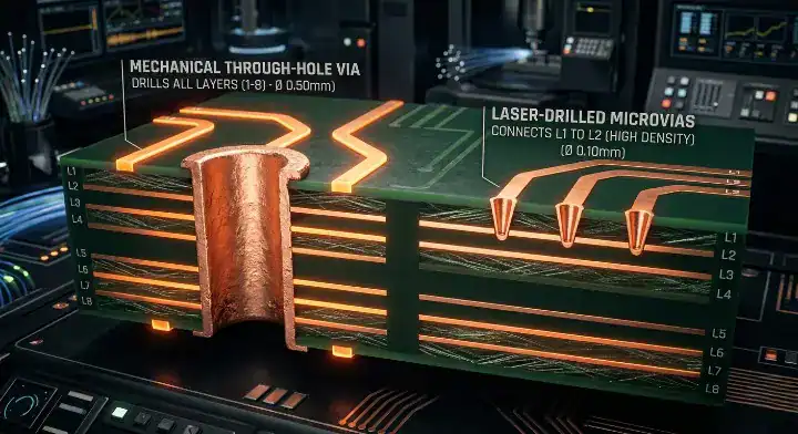
How to Calculate HDI Microvia Aspect Ratio
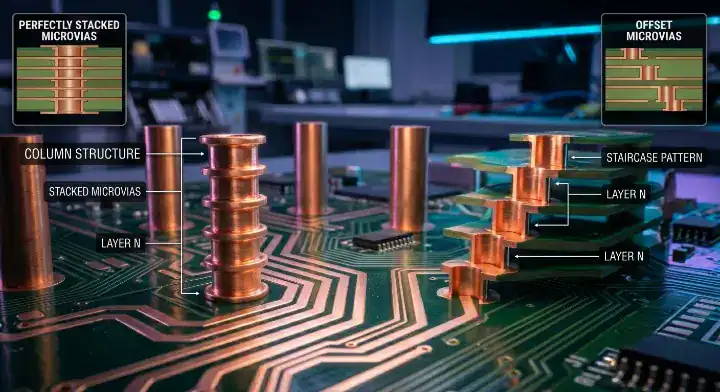
Stacked vs Staggered Microvias: Reliability, Cost and BGA Escape
Via-in-Pad Copper Fill vs Resin Fill: Which Via Gets Which
Carbon Ink PCB Pads: Design Rules for Keypad and Switch Contacts
Gerber Files for PCB Fabrication: What to Include, How to Export and Check
PCB Panelization for Assembly: Rails, Fiducials, V-Score and Tabs
How to Prevent a $4,500 PCB Redesign Due to Poor Test Access
How to Route Fine-Pitch BGA Fanout HDI PCB Like a Pro
How to Apply Ceramic PCB Design Rules: 12 DFM Checks
How to Use an HDI PCB DFM Checklist for Layout
HDI Stackup Types: How to Choose 1+N+1, 2+N+2, or ELIC PCB
How to Decide When to Use HDI PCB in Layout: 7 Signals Your Standard Multilayer Design Has Reached Its Limit
PCB Overheating: How to Find the Thermal Bottleneck
PCB Gold Fingers: Hard Gold, Thickness, Bevel and Design Rules
Engineering Change Notice (ECN) for PCBs: ECR vs ECO vs ECN, Form Fields and Process
4 Layer vs 6 Layer PCB: Stackups, Cost, Lead Time and When to Upgrade
How to Make Controlled Impedance PCB Requirements Clear
6-Layer vs 8-Layer PCB: Stackups, When to Upgrade, Cost and Lead Time
PCB Via Current Capacity: Formula, Worked Examples and Via Count
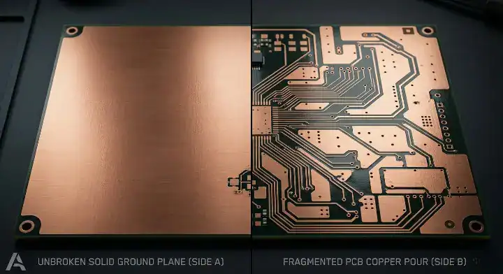
How PCB Copper Pour vs Ground Plane Choices Work
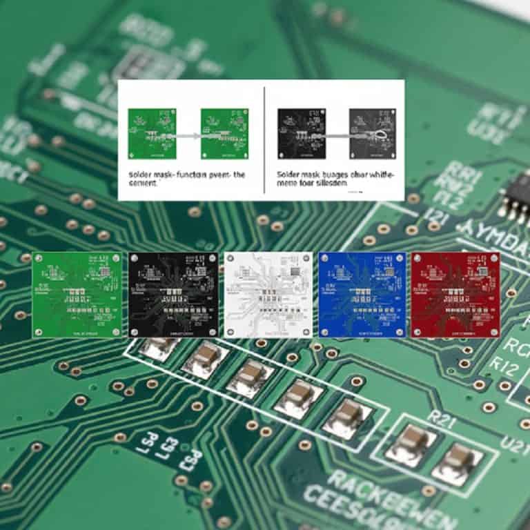
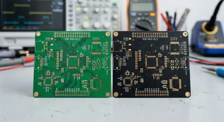
PCB Solder Mask Colors: Cost, DFM and How to Choose
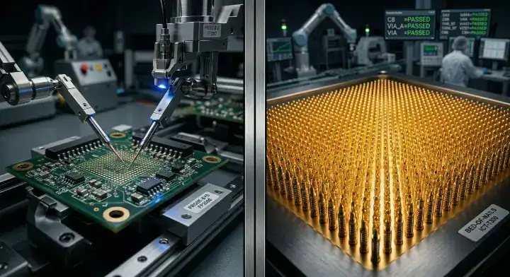
PCB Design for Test: Test Points, ICT and Flying Probe Checklist
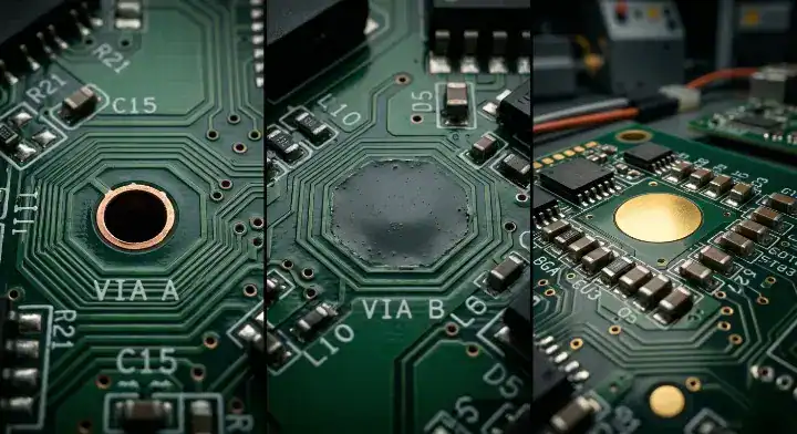
Via Tenting vs Plugging vs Filling: IPC-4761 Types and When to Use Each
HDI PCB vs Standard PCB: Cost, Routing and Reliability
How to Get PCB Stack-Up Design Right Before Fabrication
PCB Fabrication Tolerances: Which to Specify and Which to Pay For
PCB Copper Weight Cost: When Do You Actually Need 2oz?
PCB Trace Width & Spacing Guide: Rules, Charts & Calculator
2 Layer vs 4 Layer PCB: Differences, Cost, Lead Time and How to Choose
Heavy Copper PCB Design: Copper Weight, Trace Width and Layout Rules
DFM PCB Design Checklist: Fabrication, Assembly and Release
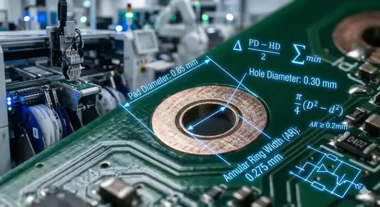
The Ultimate Guide to Annular Ring in PCB Design (With Formulas)
How to Use an Eye Diagram to Fix PCB Signal Issues
10 High Speed PCB Design Rules for Reliable AI Hardware
What Is Solder Mask? A Complete Guide to PCB Design Standards
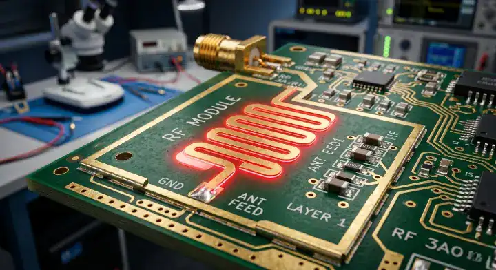
How to Avoid 7 Costly PCB Antenna Design Mistakes