
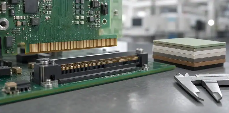
Quick Answer: A PCB edge connector bevel is a controlled leading edge for a mating socket, not a cosmetic chamfer. Define which edge and face are beveled, the required angle and extent, board thickness, finger artwork, nearby copper keepout, and the connector used for fit. Review the bevel with gold-finger plating and panel access, but do not let one substitute for the other.
Key takeaways
- Bevel geometry belongs to the mating connector interface.
- Hard-gold selection and beveling are linked but different requirements.
- Inner-layer clearance and a physical fit check prevent expensive connector damage.
An edge card can pass electrical test and still scrape, hang up, or expose copper during insertion. The most common cause is not an exotic material problem. It is an incomplete fabrication note: the connector edge is visible in layout, but the bevel side, profile, copper-free zone, and receiving inspection method were never frozen.
Table of Contents
- Decide whether the connector needs a bevel
- Name the exact board edge and face
- Control angle, extent, and stop line
- Keep copper away from the cut path
- Coordinate the bevel with plated fingers
- Use the mechanical sample as evidence
- Define incoming acceptance
- Quote the connector interface as one package
- Review the whole card-edge interface before approving a bevel
Decide whether the connector needs a bevel
Read the connector datasheet before selecting a bevel. Some sockets guide a square board edge; others rely on a tapered leading edge. A bevel is only useful when it matches the connector’s entry geometry and the board thickness used in the actual product.
The connector part number is the starting point because card sockets differ in their lead-in construction. Some use a molded mouth that accepts a square edge; others expect a bevel to guide the card past spring contacts. Board thickness, keying position, insertion direction, and required mating cycles should be checked against that connector data. A visually familiar gold-finger edge is not evidence that its bevel belongs on this design.
Connector rule: The socket data, not the appearance of the fingers, determines whether a bevel is needed.
Name the exact board edge and face
A drawing should identify the connector edge by a datum or clearly marked view, then state top-side, bottom-side, or both-side treatment. The phrase gold finger edge is not precise enough when two card edges exist or when the board can be mirrored in a panel.
Mark the edge in an enlarged drawing view with an unmistakable orientation. State whether the bevel is on the component side, solder side, or both. This matters for asymmetric contact layouts and for panels that may be rotated at routing. A callout placed next to a gold-finger row without a board-face reference can be read differently by layout, CAM, and receiving.
Orientation rule: Release cannot proceed until the bevel face is unambiguous on the fabrication view.
Control angle, extent, and stop line
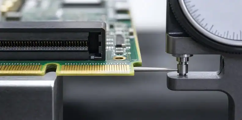
The mating interface needs more than an angle. It needs the start and stop of the bevel, its height or depth, and the transition relative to finger ends. The connector supplier’s requirement is the governing input; avoid copying a nominal angle from an unrelated edge-card design.
The bevel definition should have a measurable stop line. Show where the slope begins relative to the finger tips, how far it travels into the board, and which nominal thickness it assumes. If the mating connector permits a range of bevel angles, put the accepted range in the drawing instead of selecting an angle from a past build whose connector or thickness was different.
| Interface type | Buyer input | Fabrication confirmation |
|---|---|---|
| Card-edge socket | Entry geometry and board thickness | Bevel side, angle, extent, copper clearance |
| Gold-finger interface | Finger artwork and duty | Plating access, bevel route, finish evidence |
| Non-electrical guide slot | Mechanical section | Whether bevel is needed at all |
Keep copper away from the cut path
A bevel removes material along the edge. Inner copper that approaches the bevel can become exposed after machining, and nearby outer pads can lose their intended geometry. Define a local keepout in the released layer set, then ask CAM to confirm that the actual stackup preserves it.
Inner copper clearance deserves its own layer check. The router removes glass and resin across the bevel path, not just the outer finish. A plane edge that looks safe in a top-layer view can appear at the card edge after material is removed. The layout should reserve a verified no-copper band on every relevant layer, with particular attention to ground pours that extend automatically during a later revision.
Edge rule: Verify the copper-free band through the bevel envelope on every affected layer.
Coordinate the bevel with plated fingers
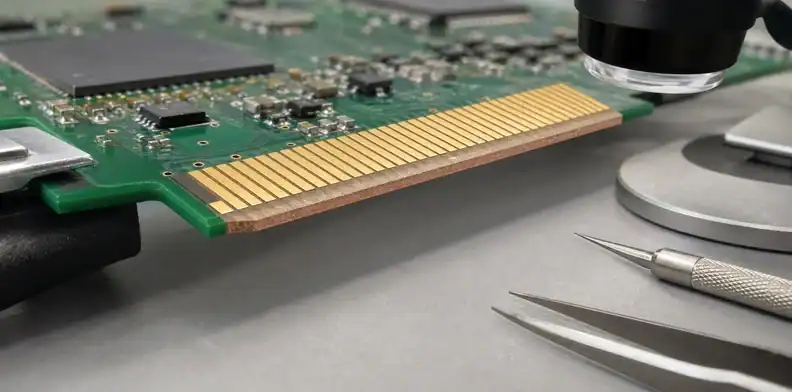
Hard gold, nickel underplate, finger length, and bevel route are separate controls. The plating feature needs panel connectivity and process access; the bevel needs a machinable edge. A change to panelization can make a once-feasible finger edge inaccessible even though the Gerber fingers did not move.
Gold-finger plating controls the contact surface, while beveling controls insertion. Panel connection bars, nickel and hard-gold areas, tape or mask boundaries, and final route sequence can affect both operations but are not one requirement. Ask the fabricator to confirm how the panels will be supported through plating and bevel machining, especially when the card edge is close to a breakaway tab.
Use the established gold-finger plating acceptance page for the contact-finish evidence, while keeping the bevel geometry as a separate connector-entry requirement.
Use the mechanical sample as evidence
For a new connector, a physical mating check is more valuable than a generic beauty photo. Verify insertion force by feel, full seating, contact wipe, and absence of visible scraping. Retain the connector part number and board revision with the first-article record.
A production sample should be inserted into the exact socket, not a similar spare connector. Check that the card starts without a snag, reaches the seating depth, and does not scrape finish from the leading fingers. Where the system sees repeated service, record the connector manufacturer and part number with the fit test. That evidence has more engineering value than an unqualified statement that the bevel looks smooth.
| Card-edge check | Evidence | Decision owner |
|---|---|---|
| Leading-face orientation | Enlarged bevel view | Connector design |
| Taper versus socket mouth | Connector data and fit sample | Mechanical engineering |
| Finger finish access | Panel-process confirmation | Surface-finish owner |
| Insertion performance | Released-socket trial | Product validation |
Fit rule: A connector insertion check is the acceptance evidence for a new card edge.
Define incoming acceptance
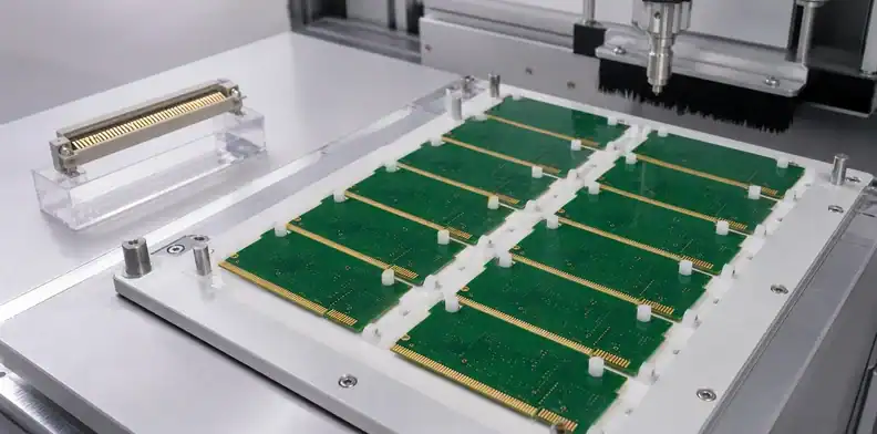
Receiving inspection can check the correct edge, visible transition, finger damage, exposed inner copper, loose fibers, and a representative mating fit. It should not attempt to infer plating thickness from appearance; that evidence belongs to the gold-finger plating report when the application requires it.
Receiving can inspect chipped laminate, exposed inner copper, damaged fingers, and the direction of the taper. It should refer plating-thickness questions to the agreed finish evidence rather than trying to infer hard-gold performance from color. A simple mating gauge or production connector is useful for a quick acceptance screen when the product cannot spare a complete host assembly.
Check the routed taper alongside edge-plating acceptance evidence before the card-edge release is locked.
Quote the connector interface as one package
Send the connector drawing, board thickness, finger artwork, bevel callout, stackup, edge keepout, expected insertion duty, and panel constraints. QueenEMS can return a DFM response that separates bevel feasibility, plating access, and any change that needs engineering approval.
For quotation, send the connector outline, edge view, finger artwork, finished thickness, plating requirement, bevel callout, and panel restrictions together. That package lets the fabricator isolate whether a concern is an insertion geometry issue, a finish-access issue, or a routing-access issue. Each result can then be resolved by the owner of the connector interface before boards enter production.
Quote rule: Resolve plating access and bevel routing as separate process questions.
Review the whole card-edge interface before approving a bevel
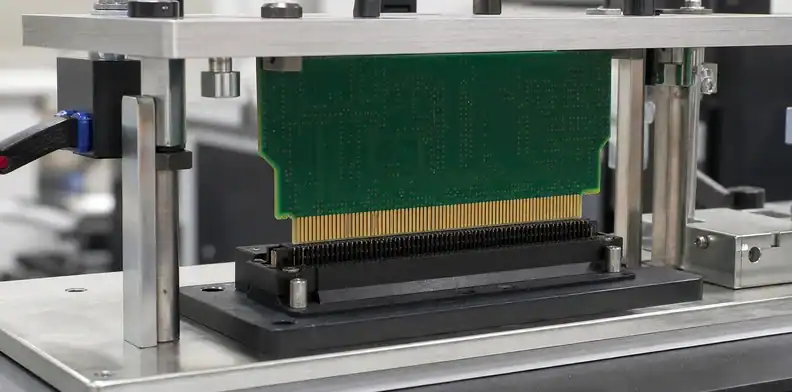
Imagine a plug-in control card with plated contact fingers on one edge and a key slot near the opposite end. The socket manufacturer specifies a lead-in chamfer for a particular nominal thickness, but the PCB revision adds a heavier copper stackup and changes the finished thickness. The bevel can still look visually correct while the card enters at a different height and the contacts touch too early. Review the connector entry profile, finished thickness tolerance, finger start position, and keying geometry together. The drawing should show the bevel from the mating direction and state which board face carries the taper. A panel operation that turns the card over can otherwise create a good-looking bevel on the wrong face, with no electrical test able to reveal the error before assembly.
Finish requirements add another layer of detail. A connector rated for repeated insertion may require nickel and hard gold on the contact zone, whereas the surrounding edge may have a different finish. The bevel route must not chip that edge or leave a transition that catches a spring contact. At the same time, the machining sequence and panel support must preserve access to the plating bars. Ask the fabricator for a process-aware answer: whether the fingers are plated, protected, and beveled in a compatible order, and whether the proposed panel arrangement changes the exposed card edge. Avoid accepting a response that simply says gold fingers and bevel are supported, because it does not confirm their relationship on this artwork.
The final acceptance test is mechanical. Insert representative boards into the released connector at the expected entry angle and check the entire travel, not merely first contact. Look for scraping at the finger tips, partial seating, laminate lift, or a keying interference near the bevel. When the interface is used in field service, record a practical sample count or agreed insertion check with the first article. This turns the bevel from an aesthetic routing note into a controlled part of the connector qualification evidence.
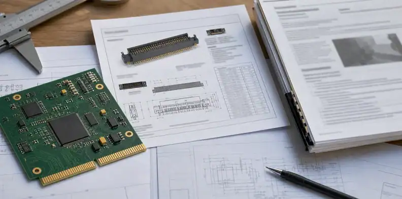
The release package should let a person who has never seen the product understand the card’s direction of travel. Begin with the connector manufacturer and part number, the required board thickness, and the expected insertion orientation. Show an enlarged edge view that marks the leading side, the beveled face, the finger area, and the taper stop line. Add the full layer keepout, because an outer-layer drawing cannot prove that an inner plane will not be exposed by machining. Then connect the bevel to the finish requirement without confusing the two: name the contact finish, nickel requirement where applicable, panel connection constraints, and the evidence requested for the intended duty. A practical production plan also says how a first article will be checked. For example, a controlled mating test may use the released socket and verify entry, seating, and visible edge condition after insertion. If a routing or plating proposal changes the edge geometry, that proposal should be compared with this controlled view, not accepted because it resembles another gold-finger product. This is how a bevel remains a defined connector interface through panelization, finish processing, and final inspection.
The bevel also has a service-life dimension. A card that is inserted once during factory assembly may tolerate a different contact and finish strategy from a module that is removed repeatedly in the field. The design owner should state that duty and the intended connector, because it affects the value of the first-article mating check. The fabricator should confirm only the edge construction and process feasibility; it should not be asked to infer lifecycle from a finger drawing. During receiving, compare the product revision with the edge view and inspect the contact zone for route damage or exposed copper. This disciplined handoff keeps later connector or panel changes from weakening a bevel that originally worked in qualification.
FAQ
Does every gold-finger board need a bevel?
No. The connector drawing and insertion geometry decide whether a bevel is required.
Can ENIG replace hard gold for a connector edge?
No. Finish selection depends on the connector duty and its specified contact system; the bevel does not decide the finish.
Why does inner copper need a keepout?
Because bevel machining can reveal inner copper at the board edge when the stackup and local clearance are not controlled.
What should the first article prove?
It should prove physical insertion and seating with the actual connector, as well as the released edge geometry.
Request an edge-card interface review
Share the connector data sheet, finished-thickness requirement, finger artwork, bevel section, and panel limitations with QueenEMS. The resulting review can distinguish insertion geometry from finish or routing-access concerns.
Sources
Written by the QueenEMS Engineering Team
Upload your files today · Free DFM check before production · Ship worldwide
Get your PCB prototypes in as fast as 24 hours. We handle FR4, Rogers, and hybrid boards up to 40 layers in volume production, with advanced builds subject to engineering review — free prototypes for 2–4 layer FR-4 boards, no minimum order.
Just upload your Gerber + BOM — we source every part, assemble, and inspect (AOI + X‑Ray) so you don't have to chase suppliers. Boards ship in as fast as 24 hours.