
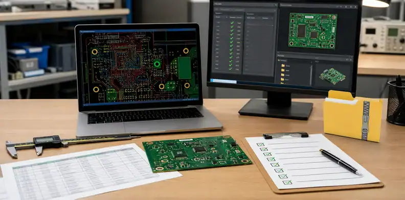
Quick Answer: An AI-generated PCB should not move from export to purchase order without a release check. The minimum review covers file completeness, DRC versus fab capability, footprint truth, stackup and impedance, Gerber/drill export, assembly data, and build evidence. Treat the AI output as a candidate design until engineering and the fabricator agree on what is being built.
The risk with an ai generated pcb is not that the layout looks unfinished. The risk is the opposite: the board can look complete while the files still hide missing drill data, generic rule settings, unverified footprints, or a stackup nobody has priced. Use this page as the hub for the AI-PCB release path. It tells you what your team can check before upload, what the factory must confirm during DFM/CAM review, and which deeper article owns each high-risk decision.
Table of Contents
- Can an AI-generated PCB go straight to a fab?
- What is the first screen before quote upload?
- Why does DRC not equal manufacturability?
- How should footprints and pin mapping be verified?
- Who owns stackup and impedance?
- Which fabrication files must be present?
- What can the factory catch during CAM?
- What evidence should be requested?
- When is the prototype ready for production?
Can an AI-generated PCB go straight to a fab?
No. Uploading exported Gerbers is technically possible, but ordering from the export button makes every AI assumption a production assumption.
A generated layout may have copper, holes, and a board outline, yet still lack a named revision, controlled stackup, assembly file set, or acceptance evidence. The first release question is whether the package describes the intended product, not merely whether the CAD tool can create files.
Hold the order when electrical intent, part orientation, board thickness, finish, or test expectation lives only in chat history. Those items need to be visible in drawings, notes, BOM/CPL files, or RFQ text before a quote can be compared fairly.
For an export-only AI board, the release note should identify the final CAD revision, exported ZIP name, and which checks were performed outside the design tool. The practical reason is that a board can be quoted from the wrong iteration even when the current layout looks correct.
For export-only AI boards, the hold record should name the Gerber/ODB++ archive, viewer discrepancy, and design owner who confirms whether the files are orderable.
Release rule: An AI file is order-ready only after the package states what to build, what the factory may change, and what evidence will prove acceptance.
What is the first screen before quote upload?
Start with a viewer check and a package inventory before detailed engineering debate.
Open the final ZIP outside the design tool and confirm copper layers, solder mask, silkscreen, outline, NC drill, drill map, paste layers when assembled, BOM, centroid/CPL, and fabrication notes. This catches missing export settings that a green local DRC cannot reveal.
Then compare the visible board definition with the quote request: layer count, copper weight, thickness, finish, panel requirement, controlled impedance, special material, and assembly scope. If the quote form says one thing and the files say another, the supplier will either stop or quote the wrong work.
For a first quote upload, keep a screenshot or viewer report beside the file list so purchasing can see what was actually sent. The practical reason is that email attachments and renamed ZIP files can hide a missing drill or older outline.
For the first quote upload, write the missing item in the RFQ cover note, such as stackup source, board outline file, drill chart, or controlled feature.
AI-PCB release screen:
| Check area | Buyer action | Factory action | Stop condition |
|---|---|---|---|
| Package inventory | Open ZIP in a viewer | Confirm CAM-readable files | Missing drill or outline |
| Rules | Compare loaded limits | Run DFM/CAM checks | Generic DRC deck |
| Footprints | Match MPN and orientation | Review assembly fit | Package mismatch |
| Evidence | Define required records | Price the evidence scope | Quote excludes proof |
Why does DRC not equal manufacturability?
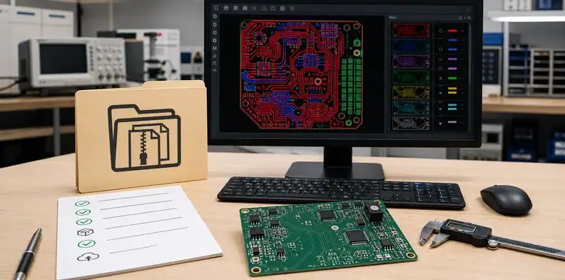
DRC checks the rules loaded into the CAD database; manufacturability depends on the supplier’s real process window.
An AI autorouter can pass a default 5 mil spacing rule while the selected copper weight, mask registration, drill aspect ratio, or annular ring target needs more room. The clean result proves only that the software found no violation against its own rule deck.
The deeper PCB DRC vs DFM limits article owns that distinction. In this hub, the action is simple: load supplier limits before routing where possible, and still ask for DFM/CAM review when the design uses tight copper, fine vias, edge copper, or unusual stackup.
For a DRC-clean generated route, ask whether the rule source is a supplier capability table, a CAD default, or a copied project setting. The practical reason is that the answer decides whether the clean result deserves trust or another DFM pass.
Put the violated fabrication limit back into the CAD rule set, then re-export the route with a note identifying the changed clearance or drill constraint.
DFM signal: A passing DRC is a screening result, not a supplier acceptance record.
How should footprints and pin mapping be verified?
Verify the exact manufacturer part number against the datasheet and a physical package view.
AI-generated symbols and library choices can look believable while the pad pitch, exposed pad, pin 1 mark, polarity, or package suffix is wrong. A board with wrong footprints can fabricate perfectly and fail only when assembly starts.
For the detailed process, use AI PCB footprint verification. Before this hub article releases an order, require a symbol-to-footprint check, a 1:1 print or mechanical fit check, polarity review for diodes and ICs, connector keying, and BOM package-code match.
For a mixed BOM/CAD handoff, compare the CAD footprint name with the BOM manufacturer part number and the CPL rotation before assembly pricing. The practical reason is that the bare board can be good while the assembly package is unusable.
For mixed BOM and CAD data, stop at the part line: either approve the footprint/MPN pair or revise the library before quote release.
Who owns stackup and impedance?
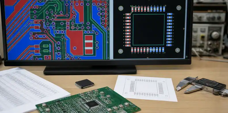
Engineering owns the impedance requirement; the fabricator owns the buildable stackup that can meet it.
A drawn 50 ohm trace is only geometry until the routing layer, return plane, dielectric spacing, laminate Dk, finished copper, mask coverage, and tolerance are defined. AI tools often assume a generic 1.6 mm FR-4 stackup that does not match the actual press cycle or laminate stock used by the supplier.
When controlled impedance matters, link the quote to code-generated PCB stackup control and provide target impedance, layer, trace geometry, net names, tolerance, and whether coupon/TDR evidence is required. Without those fields, the quote cannot distinguish a visual trace from a controlled trace.
For a controlled-impedance net, store the impedance target beside the stackup request instead of leaving the trace width as the only clue. The practical reason is that a fabricator cannot price a controlled build from geometry alone.
If impedance geometry moves, send engineering the old width, proposed width, dielectric change, and coupon plan before refreshing fabrication data.
Factory review boundary:
| Item | Factory can review | Engineering must own |
|---|---|---|
| Copper spacing | Etch and yield window | Signal or creepage purpose |
| Stackup | Buildable material and thickness | Impedance target |
| Footprint | Assembly clearance questions | Pin mapping truth |
| Test | Fixture feasibility | Functional acceptance |
Stackup rule: The supplier may adjust geometry for a buildable stackup, but engineering must approve any change that affects electrical intent.
Which fabrication files must be present?
A release package needs more than top and bottom copper.
For bare-board fabrication, include every copper layer, mask and legend artwork, rout or outline data, Excellon drill, tool map, fabrication notes, and revision identity. For assembly, add paste, BOM, centroid/CPL, polarity notes, panel preference, test request, and any assembly exclusions.
The spoke article on AI PCB Gerber review before quote goes deeper into export traps. The hub decision is whether the factory can quote from real manufacturing files rather than screenshots, design-tool project files, or an ambiguous drawing alone.
For a Gerber package created after many AI iterations, include one clear revision label in the ZIP and remove obsolete exports from the same folder. The practical reason is that CAM may otherwise review files from different design states.
For Gerbers after many AI iterations, compare layer timestamps and reject any archive that mixes old drill, new copper, or stale outline data.
What can the factory catch during CAM?
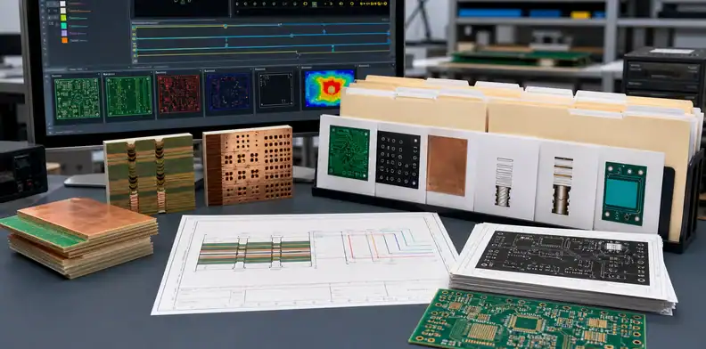
The factory can catch process conflicts, but it cannot infer product intent that is absent from the files.
CAM review can flag annular ring risk, mask slivers, copper-to-edge clearance, board-outline ambiguity, stackup feasibility, copper balance, panelization questions, and drill limitations. It cannot know that a generated connector pinout matches your cable, firmware loader, or test fixture.
Keep a clear boundary in every response to supplier questions. Approve cosmetic cleanup and tooling additions differently from copper edits, drill changes, stackup substitutions, material changes, or assembly substitutions, because those can change the product.
For a supplier DFM question, separate tooling cleanup from design-changing edits before approval. The practical reason is that a small CAM change can alter copper, drill, or stackup intent if the boundary is not named.
Close a supplier DFM question with the exact CAM mark, accepted geometry, and whether the next export must change.
Responsibility call: Let CAM fix manufacturability only after engineering knows whether the edit changes function, fit, or acceptance.
What evidence should be requested?
Evidence should be planned before the order, not requested after a dispute appears.
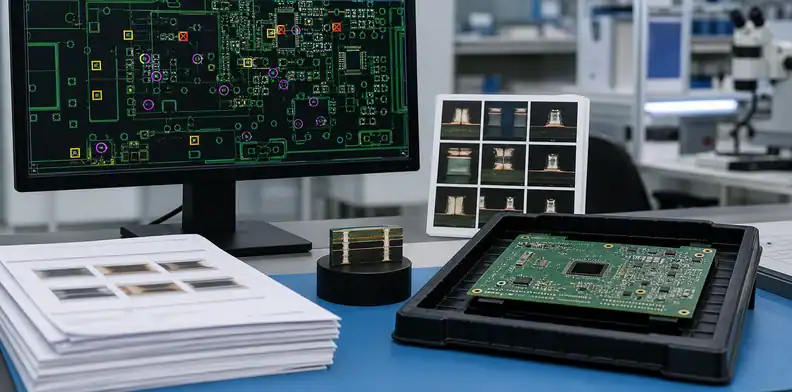
Electrical test proves opens and shorts, not application function. Microsection can document plated-hole structure; TDR coupons support controlled impedance; AOI and X-ray help with assembly and hidden joints; a COC is useful only when it ties back to the agreed order and records.
Use AI PCB manufacturing evidence when the board has hidden vias, impedance, high density, safety relevance, or first production risk. A cheaper quote that excludes coupons, reports, or inspection records is not the same scope as a quote that includes them.
For a prototype meant to become a pilot lot, decide which records must follow the lot before the PO is placed. The practical reason is that after fabrication starts, missing coupons or inspection records may no longer be recoverable.
A prototype moving into a pilot lot needs frozen Gerbers, BOM/CPL, stackup, test limits, and accepted DFM changes in one package.
When is the prototype ready for production?
A prototype is production-ready only after bench fixes become controlled specifications.
Freeze revision, stackup, material assumptions, solder finish, stencil needs, reflow limits, test points, programming method, inspection standard, and supplier change rules. Hand rework, lab jumpers, or manual touch-up should become design changes or documented process instructions before volume.
The transition article on AI PCB prototype to production checks covers the pilot path. In the hub, the practical stop sign is any working prototype that still depends on memory, a single technician, or undocumented substitutions.
For a volume-release decision, turn rework notes, test shortcuts, and hand-solder lessons into controlled drawings or process notes. The practical reason is that production fails when prototype memory becomes the hidden specification.
The response for a volume-release decision should make the next step obvious to CAM, fabrication, assembly, or receiving without asking anyone to interpret chat history.
Production call: Do not release volume until the design can be built, inspected, and repeated without hidden prototype knowledge.
For release review, send QueenEMS the final ZIP, BOM/CPL, stackup notes, requested evidence, and unresolved DFM questions through the QueenEMS contact page. Mark the revision name, order quantity, frozen decisions, and items that still need engineering approval.
FAQ
Can I send AI-generated Gerbers straight to fabrication?
No. Send them only after viewer, DRC/DFM, footprint, stackup, Gerber, BOM/CPL, and evidence checks are full.
What is the fastest useful check before ordering?
Open the export in an independent viewer and verify layer set, outline, NC drill, units, revision, and assembly files.
Will the PCB supplier catch AI design mistakes?
Only process-related mistakes. Electrical intent, pin mapping, firmware behavior, and product acceptance must come from the buyer’s engineering record.
How do I know if an AI-generated PCB package is ready for quote?
It is ready for quote when the fabrication files, stackup intent, critical footprints, controlled features, and evidence requests agree with the same revision. If any one of those items still lives only in a chat prompt or screenshot, hold the RFQ until it is written into the order package.
Sources
Written by the QueenEMS Engineering Team
Upload your files today · Free DFM check before production · Ship worldwide
Get your PCB prototypes in as fast as 24 hours. We handle FR4, Rogers, and hybrid boards up to 40 layers in volume production, with advanced builds subject to engineering review — free prototypes for 2–4 layer FR-4 boards, no minimum order.
Just upload your Gerber + BOM — we source every part, assemble, and inspect (AOI + X‑Ray) so you don't have to chase suppliers. Boards ship in as fast as 24 hours.