

Quick Answer: PCB DRC vs DFM is the difference between a loaded software rule deck and the supplier’s physical process window. A clean DRC result does not prove etch compensation, drill wander, solder mask registration, copper weight, or assembly clearance. For AI-routed boards, use supplier capability rules before routing and request DFM/CAM review before quote release.
The most expensive misunderstanding in an AI-routed board is treating a green DRC report as permission to buy. The software checked geometry against rules, but it did not prove that the chosen fabricator can etch, drill, plate, mask, and assemble the board at acceptable yield. This article stays on that boundary. It explains what DRC can prove, what DFM must still review, and how to turn supplier capability into rules that reduce quote holds.
Table of Contents
- Does passing DRC mean the board is manufacturable?
- What exactly does DRC check?
- What does DFM add after DRC?
- Why do AI-routed boards fail after clean rules?
- How should supplier capability become CAD rules?
- How do etch and copper weight change the answer?
- What still needs DFM review before quote?
- What should the RFQ say?
Does passing DRC mean the board is manufacturable?
No. It means the CAD database follows the rule deck that was active during the check. If an AI tool or autorouter used generic minimums, the report can be clean while the chosen copper weight, drill size, aspect ratio, mask web, or edge clearance is outside the fabricator’s comfort zone. Keep the AI-generated PCB release checklist nearby when a rule-screen result has to become an order-release decision. DRC is especially weak when the rules were copied from a template rather than built from the selected supplier’s capability table.
Use DRC as a design-side screen. Use DFM as the manufacturing-side review that considers etching, plating, lamination, drilling, solder mask, surface finish, and assembly access.
For a clean DRC report from an AI autorouter, save the rule deck version and the supplier capability source used to create it. The practical reason is that otherwise the report proves software consistency but not supplier fit.
For a clean DRC report, record which rule source was used and which fabrication capability still needs supplier confirmation, such as drill aspect ratio or solder mask web.
Decision rule: A green DRC report can start supplier review, but it cannot replace supplier DFM approval.
What exactly does DRC check?
DRC checks measurable database relationships such as clearance, width, hole size, annular ring, and component courtyard. Use AI PCB footprint verification when the DRC result looks clean but the package geometry still needs library proof.
Those checks are valuable when the rule values match the board being ordered. For example, a 5 mil trace/space rule can protect a simple 1 oz FR-4 prototype, but the same setting may be too aggressive after heavier copper, higher voltage spacing, or a different solder mask process is selected.
AI-generated boards often inherit a single global minimum. Power nets, high-speed nets, connector regions, and high-voltage areas need different constraints, so one clean report can hide several classes of risk.
For a board routed at a single global minimum, review power, connector, impedance, and high-voltage regions as separate rule classes. The practical reason is that one minimum can be legal yet inappropriate for several net families.
For a board routed at one global minimum, list the copper weight, layer class, and feature family that makes that limit unsafe for real fabrication.
DRC vs DFM scope:
| Question | DRC answers | DFM answers |
|---|---|---|
| Is the spacing below the loaded rule? | Yes or no | Whether the process can hold it |
| Is the drill allowed? | Database minimum | Wander, plating, aspect ratio |
| Is the mask clearance legal? | Rule comparison | Registration and mask dam risk |
| Is the stackup real? | Usually no | Material and press plan |
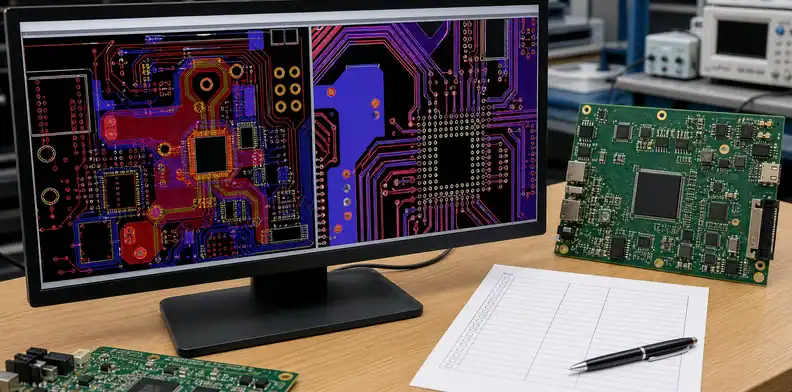
A useful DRC setup also records where each limit came from. Some values belong to the EDA tool default, some come from a board house capability table, and some are project choices such as copper weight, surface finish, or connector clearance. If those sources are mixed without labels, the clean report becomes hard to defend when a supplier asks why a 4 mil gap, a via annular ring, or a solder mask web was accepted.
What does DFM add after DRC?
DFM tests whether the design can survive real fabrication and assembly steps. A fabricator looks at etch compensation, drill registration, plating thickness, lamination movement, mask registration, copper balance, rout tolerance, panelization, surface finish, and inspection method. The code-generated PCB stackup control article owns the impedance side of that DFM conversation. These are process behaviors, not just geometric distances inside the CAD database.
The same Gerber can be easy in one process and marginal in another. That is why an online auto-quote may accept a file while engineering review later raises a CAM question.
For a supplier DFM response, ask the CAM engineer to mark layer, feature, and reason for every hold. The practical reason is that generic hold comments are hard to turn into CAD-rule improvements.
A supplier DFM response that changes copper, drill, mask, or outline geometry belongs in the CAD constraint record before a fresh file export.
Process call: DFM turns CAD geometry into a supplier-specific build question.
Why do AI-routed boards fail after clean rules?
AI routing tends to optimize connectivity and density before it understands manufacturing preference.
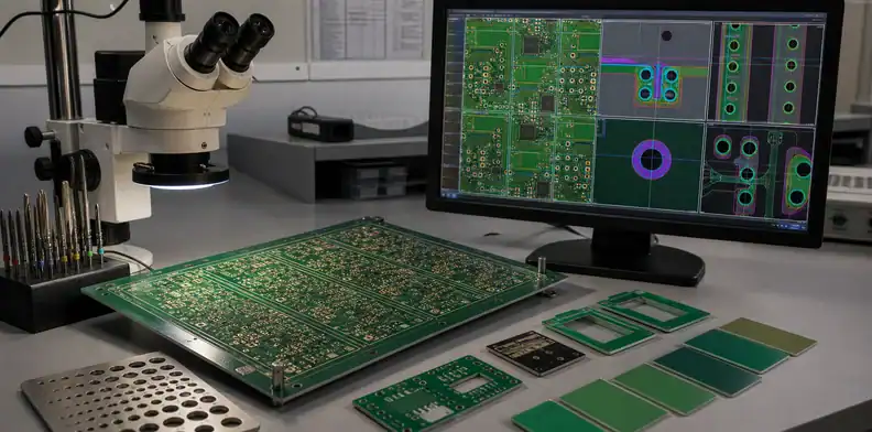
Common failure modes include using the narrowest trace on every net, placing vias near pads without assembly intent, routing copper too close to the edge, leaving mask slivers between pads, and creating acute copper pockets that increase etch risk. The board can still satisfy the literal local rules.
Review the design for patterns, not only single violations. A dense via field, long same-width power path, or tightly packed connector escape can signal process risk even when no one object is illegal.
For a dense via escape, look at via fields as a process pattern instead of isolated holes. The practical reason is that drill registration and plating yield can be weak even when each via clears the local rule.
For dense via escape, decide whether the fanout can be opened, the drill can change, or the supplier needs a different build class.
How should supplier capability become CAD rules?
Convert the supplier’s capability table into net classes and region rules before final routing.
Set values for trace width, spacing, via drill, via pad, annular ring, solder mask clearance, mask dam, copper-to-edge, mechanical slots, and aspect ratio. Then separate power, impedance, high-voltage, connector, and fine-pitch escape rules instead of relying on one board-wide minimum.
When the supplier returns CAM feedback, update the CAD rule set before the next AI or autorouter pass. Otherwise the same tool will keep regenerating the same manufacturability problem.
For a capability-table update, transfer the supplier’s recommended values into the CAD project before rerouting. The practical reason is that using the same AI setup again recreates the same rejected geometry.
When the capability table changes, update the rule deck source date and leave a quote note explaining which prior limit was retired.
AI routing risk patterns:
| Pattern | Why it passes DRC | DFM concern |
|---|---|---|
| All nets at minimum width | Width is legal | Current and yield margin |
| Dense via fields | Individual vias pass | Drill and plating crowding |
| Copper near outline | Edge rule may be loose | Routing tolerance |
| Fine mask webs | Mask rule is generic | Registration loss |
Capability check: Supplier feedback should change the rule deck, not live only in an email thread.
Translate repeated supplier comments into rule names that a designer can understand later. Instead of a generic note such as fab said spacing is tight, create separate limits for inner-layer copper spacing, outer-layer etch compensation, solder mask dam, drill-to-copper, and board-edge clearance. That keeps a one-time CAM warning from turning into a recurring quote delay on the next revision.
How do etch and copper weight change the answer?
Finished copper is affected by copper weight and etch compensation, so artwork width is not the whole story.
A light 0.5 oz signal layer may support finer geometry than a 2 oz power layer because heavier copper needs more compensation and spacing margin. Supplier-specific compensation can move by roughly 0.5 to 2.0 mil per side depending on copper weight and process control.
Do not set one minimum for every copper layer. Ask the supplier whether the target line/space applies to the exact copper weight, finish, and stackup in the quote.
For a heavier-copper revision, recheck finished spacing and trace width after the copper weight changes. The practical reason is that the artwork that passed on thin copper may need more etch margin.
For heavier copper, capture the new etch spacing, thermal relief, mask clearance, and current path limit in the revision note.
What still needs DFM review before quote?
Request DFM review for features that depend on process behavior or supplier preference.
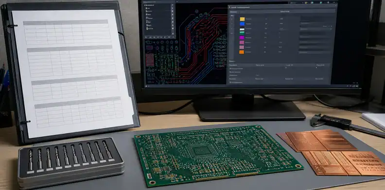
The list includes tight line/space, small annular rings, high aspect ratio drills, holes close to copper, mask slivers, fine-pitch pads, edge copper, impedance layers, copper balance, controlled stackup, and unusual outlines. For assembly, include component spacing, polarity, heat-sensitive parts, and reflow constraints.
When CAM proposes a change, classify it. Tooling tabs and fiducials may be routine; copper edits, drill changes, material substitutions, or stackup movement need engineering approval.
For a CAM-proposed edit, record whether the edit touches copper, hole size, solder mask, board outline, or only documentation. The practical reason is that only the last category should be approved without engineering review.
Close a CAM-proposed edit by saving the before/after feature and the buyer approval that allows tooling to proceed.
Capability fields to load:
| Rule field | Example value type | Owner |
|---|---|---|
| Line/space | mil or mm by copper weight | Fabricator |
| Drill and annular ring | finished drill and pad | Fabricator |
| Impedance | 50 ohm, 90 ohm, 100 ohm targets | Engineering plus fabricator |
| High voltage spacing | creepage/clearance requirement | Engineering |
Release rule: The quote should freeze which DFM changes are allowed automatically and which require written approval.
What should the RFQ say?
The RFQ should name the rule source and ask the supplier to report any process conflict before production.
A useful note is specific: state the CAD rules were set from the attached capability target, list the controlled exceptions, and ask for DFM/CAM comments on copper, drilling, mask, stackup, and assembly fit. Attach the DRC report only as support, not as proof of manufacturability.
For QueenEMS review, send the Gerber or ODB++ package, rule report, stackup target, copper weights, drill table, and any high-risk screenshots through the QueenEMS contact page.
For a release RFQ, include DRC output as background and ask for a supplier-specific DFM disposition. The practical reason is that the supplier needs permission to raise manufacturing risk rather than silently quote around it.
A release RFQ is controlled when CAD rules, supplier exceptions, quote assumptions, and approval owner all point to the same revision.
RFQ signal: Ask for process conflicts by feature and layer, not for a vague manufacturability opinion.
For manufacturability review, upload the rule report, Gerber or ODB++ export, copper weight, drill table, supplier limits, and pending fabrication questions through the QueenEMS contact page. State which CAD limits are frozen and which supplier findings may return for engineering approval.
The RFQ should separate known design intent from supplier review requests. State which limits are frozen by engineering, which features may be adjusted by CAM with approval, and which findings should come back as questions before tooling. That structure helps purchasing compare quotes because one supplier is not silently assuming an exception while another is pricing the controlled geometry.

FAQ
Does passing DRC mean my PCB is ready for fabrication?
No. It only proves the board passed the active software rules, not the supplier’s DFM process window.
Why did a fab reject a board after DRC passed?
The loaded rules were probably generic, incomplete, or more aggressive than the fabricator’s copper, drill, mask, or assembly limits.
Should I run DRC before sending files to QueenEMS?
Yes. Run DRC first, then send the DRC report with Gerber or ODB++, stackup, copper weight, and any known process-risk areas for DFM review.
How do I know if DFM feedback should change my CAD rules?
Change the CAD rules when the supplier feedback identifies a repeatable capability limit such as spacing, annular ring, copper balance, solder mask clearance, or drill aspect ratio. A one-time exception can stay in the quote record, but a normal production limit belongs in the design rule set.
Sources
Written by the QueenEMS Engineering Team
Upload your files today · Free DFM check before production · Ship worldwide
Get your PCB prototypes in as fast as 24 hours. We handle FR4, Rogers, and hybrid boards up to 40 layers in volume production, with advanced builds subject to engineering review — free prototypes for 2–4 layer FR-4 boards, no minimum order.
Just upload your Gerber + BOM — we source every part, assemble, and inspect (AOI + X‑Ray) so you don't have to chase suppliers. Boards ship in as fast as 24 hours.