
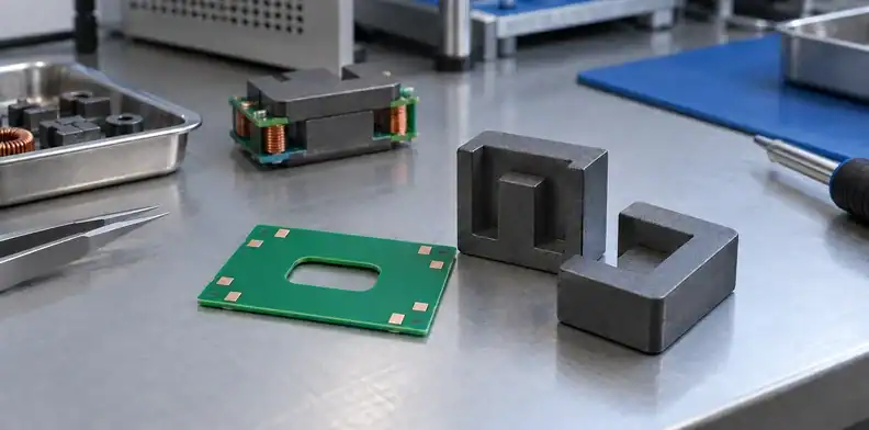
Quick Answer: Approve a planar transformer PCB against the actual core drawing, finished winding stack and layer-by-layer electrical connections. Include insulation sheets, spacers and retention features that occupy the assembly window. Fabrication records verify the winding board; magnetic and isolation performance require the specified core-installed assembly and operating conditions.
A planar transformer PCB places windings in patterned copper layers around a magnetic core. Buying the board therefore involves more than matching a layer count and an outline. Its finished geometry must fit the core, its interconnections must reproduce the winding diagram, and its insulation must remain consistent with the complete magnetic assembly.
An electrically plausible winding can become an unusable part when the fabricated stack is too tall, a terminal obstructs assembly or a supplier changes a critical dielectric. Start the purchase review with the board-core interface and keep it connected to the magnetic design. A quotation for a winding board and a quotation for a complete transformer also need separate acceptance boundaries.
Table of Contents
- Choose an integrated or separate winding PCB
- Fit the finished winding stack inside the core
- Describe winding connections layer by layer
- Review copper for the specified waveform
- Preserve the primary-to-secondary insulation system
- Put vias and terminals on the winding map
- Reconcile magnetic needs with fabrication tolerances
- Learn from a published core-window mismatch
- Test the winding board and the magnetic assembly
- Order the winding PCB with a controlled assembly boundary
Choose an integrated or separate winding PCB
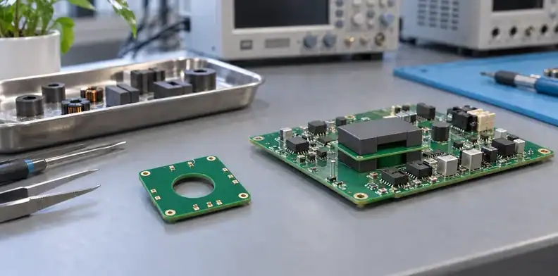
Choose the physical winding arrangement before fixing the board scope. The windings may occupy layers of the main circuit board, a separate multilayer winding board or several boards assembled with specified insulation. Each arrangement changes the parts, connections and approval work in the purchase.
A planar transformer PCB also differs from a generic spiral coil. The core, primary and secondary windings, connection polarity and insulation paths form one magnetic component. The spiral-coil fabrication discussion supports patterned-coil manufacturing; the transformer review adds these coupled assembly requirements.
| Winding arrangement | What purchasing orders | Engineering decision to resolve | Assembly boundary |
|---|---|---|---|
| Windings integrated into the main PCB | A main board containing the winding layers | Whether the whole board should use that construction | Core installation and final board-level qualification |
| Separate multilayer winding PCB | A dedicated winding board plus the main board | Interboard terminals, space and component ownership | Winding-board assembly before connection to the system |
| Several winding boards with insulation | Identified boards and intervening materials | Total stack, registration and interconnections | Controlled stacking, core retention and terminals |
| Complete supplied magnetic component | A defined transformer part or assembly | Required electrical, mechanical and isolation evidence | Supplier’s component boundary and system integration |
An integrated arrangement can avoid a separate winding-board connection while extending its layer requirements across the main board. A separate winding board can isolate the magnetic fabrication task, but introduces its own terminals and assembly operations. Compare the real constructions and quantities rather than assuming either has a lower total cost.
Power Integrations’ APEC presentation on planar transformer design shows several winding and insulation arrangements. Treat them as architecture options. Select and qualify the construction intended for the product, including all separately supplied pieces.
Fit the finished winding stack inside the core
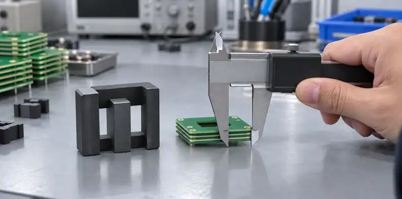
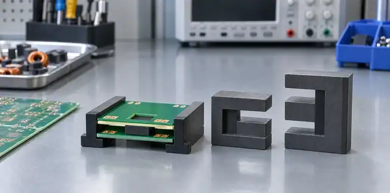
Compare the maximum finished assembly thickness with the space available in the specified core construction. Nominal PCB thickness is one contributor. The core window also has to accommodate the intended insulating materials and assembly geometry.
Use the actual core drawing
Identify the core part, material designation, revision and mating arrangement. Use its drawing to locate the centre leg, winding window, board openings and relevant mounting surfaces. Show which features locate the board relative to the core.
Review the opening around the centre leg against the finished board outline and manufacturing variation. A core that passes through an unpopulated coupon may meet a different obstruction when terminals, adhesives or retention hardware are installed. Keep these items in the assembly view.
A core supplier’s nominal window dimension should be interpreted with its tolerances and mating configuration. The magnetic designer and mechanical reviewer should agree how much space the chosen assembly requires and how that fit is checked.
Include every item between the core halves
Build a thickness budget for the region occupied by the windings. Use specified maximum or agreed controlled values for the relevant items, without silently replacing them with nominal catalogue values.
| Item in the occupied window | Information to record | Physical check |
|---|---|---|
| Finished winding PCB | Thickness range at the relevant region | Approved stack and representative board measurement |
| Outer surface layers | Mask or other applicable surface build | Inclusion in the finished dimension |
| Separate insulation sheets | Material, placement and supplied thickness | Installed sheet stack and overlap |
| Spacers or adhesive regions | Defined position and assembled thickness | Retention and spacing arrangement |
| Core mating and assembly space | Available window and intended clearance | Fit using the specified core configuration |
The finished-board thickness review addresses the fabrication dimension. For the transformer, connect that dimension to the occupied window and the permitted assembly method.
Describe winding connections layer by layer
Supply a winding diagram and a layer map that identify the same electrical connections. The number of PCB layers does not state the turns ratio, winding polarity or whether two patterned layers connect in series or parallel.
For each winding segment, identify its physical layer, direction, start and finish connections. Show the vias or terminals that connect it to another segment. A reviewer should be able to follow a conductor from the input connection through the intended turns and back to its assigned endpoint.
The following table is an illustrative document schema. It lists fields to populate from an approved magnetic design, not a tested winding construction or suggested turns count.
| Winding-map field | What to enter from the design | Cross-check against artwork |
|---|---|---|
| Physical layer identity | Fabrication layer name and viewing orientation | Export order and correct board side |
| Electrical winding identity | Primary, secondary or named auxiliary winding | Net assignment and isolation boundary |
| Start and finish | Connection references and polarity convention | Terminal location and conductor direction |
| Layer relationship | Series continuation or parallel segment | Via/pin connections and actual path |
| Turns and geometry | Approved turns per segment and conductor geometry | Pattern around the core leg |
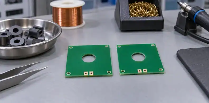
In an illustrative separate-board review, two boards may each contain part of a primary winding. Their mechanical stacking order does not establish their electrical relationship. The assembly document must show the connections and polarity when the boards are installed.
Parallel copper layers also need an explicit connection scheme. Identify where the paths join and the geometry through which current reaches them. A drawing note that says “parallel layers” cannot resolve an omitted endpoint or a connection to the wrong physical layer.
Bind the map to the same artwork revision as the fabrication order. When CAM proposes a layer-order or connection change, have the magnetic design owner review its electrical meaning before accepting the revised files.
Review copper for the specified waveform
Choose winding copper with the magnetic designer using the intended operating waveform. DC resistance helps describe the conductor, but switching-frequency winding loss also depends on the magnetic field and current distribution.
TI’s original Designing Planar Magnetics paper discusses high-frequency current distribution and winding arrangements. It also distinguishes the loss behaviour of some transformer arrangements from gapped-core inductor and flyback constructions. These mechanisms require a design-specific review.
DC resistance is one input
Record the winding current waveform, frequency range and relevant operating states alongside the conductor geometry. Peak and RMS current describe different aspects of the duty, and the core and circuit establish the excitation that the winding actually sees.
Changing copper thickness can alter fabrication constraints and the high-frequency loss calculation. A lower calculated DC resistance alone cannot approve that change. Ask the magnetic designer which finished-copper dimensions and variations the loss assessment assumed.
Use the heavy-copper manufacturing review when thick conductors affect etching, spacing or board construction. Keep the winding-specific electromagnetic assessment with the transformer design rather than applying a general trace-current example.
Interleaving changes more than leakage
Review a proposed primary-secondary layer arrangement for leakage, winding loss, capacitance and insulation requirements together. Interleaving can improve magnetic coupling while changing the electric-field geometry between windings. It does not provide a universal optimum across these requirements.
A fabrication substitution that moves a secondary layer, changes its overlap or alters the dielectric can affect more than board thickness. Identify the electrical quantities that need recalculation or measurement when the stack changes.
For a gapped-core design, include the gap location and nearby conductors in the assessment. Approval of another transformer with similar layer count does not establish equivalent winding loss under a different field distribution.
Preserve the primary-to-secondary insulation system
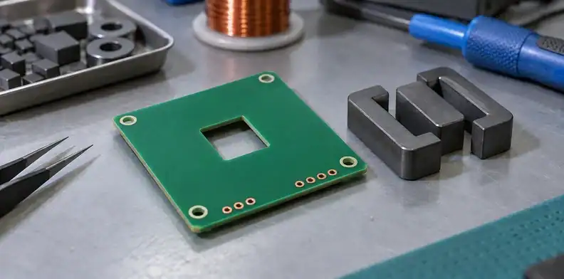
Identify the complete insulation paths between the relevant circuits in the installed component. The review includes dielectric within a multilayer board, exposed surface routes, board openings, separate insulating pieces and nearby core or retention hardware.
Assign working voltage, required insulation function and applicable product requirements through the responsible design authority. These inputs determine the construction and tests; a generic PCB dielectric-strength value cannot establish acceptance of the complete transformer.
Show where primary and secondary copper approach board edges and openings. Include exposed via pads, terminals and assembly hardware that can change the surface route. The board copper-to-edge feature discussion addresses manufactured geometry; transformer insulation approval still depends on the entire specified assembly.
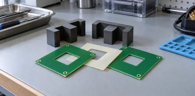
In a stacked-board arrangement, record the intervening insulation material, its orientation and the overlap needed by the design. The board thicknesses and the separate barrier are distinct items. A purchasing substitution of either requires a review of the insulation and mechanical assumptions it changes.
Slots can alter surface routes and physical clearances, but their presence alone establishes no general compliance result. Use the actual dimensions, tolerances and assembly conditions for the intended insulation assessment. Keep copper changes and cutout changes connected to that review.
Require proposed alternate constructions to identify their difference from the approved assembly. A supplier can offer a practical manufacturing alternative; the product’s electrical and insulation authority must decide whether the supporting evidence remains applicable.
Put vias and terminals on the winding map
Review every conductive transition that joins winding segments or brings them to the external circuit. Vias, terminal pins and soldered connections belong on the same map as the planar copper, with their physical positions visible.
A via group connecting parallel layers needs clear layer participation and local copper geometry. A group that looks substantial from above may include pad necks or layer connections that carry current differently. Avoid assigning winding capability from total via count alone.
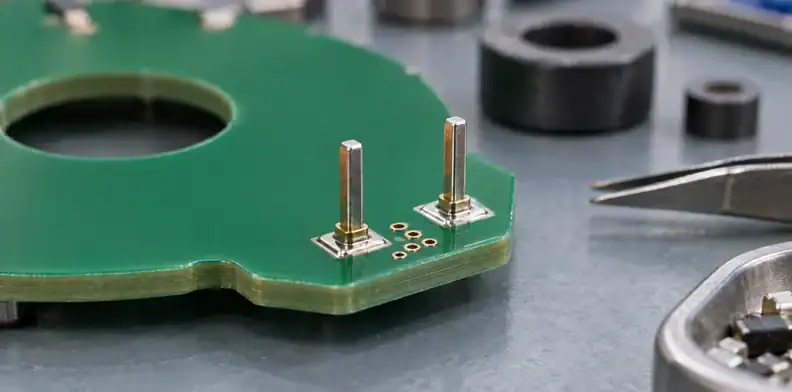
Show which through-hole features connect electrically and which provide mechanical location. A pin used to join several separate winding boards needs a specified fit and assembly sequence for each board it passes through. Its installed height must remain compatible with the core and other component clearances.
When a terminal uses an elongated opening, resolve the opening shape and finished dimensions explicitly. The manufactured plated-slot specification supports that PCB feature. The transformer drawing additionally identifies the terminal’s winding assignment and position in the installed assembly.
Check endpoint placement against the insulation route. Moving a terminal to ease solder access can shorten a primary-secondary surface path or bring a pad closer to the core hardware. Send the revised geometry back through the relevant electrical and mechanical reviews.
For a pilot using separate winding boards, inspect the interconnections before closing the core assembly. Decide which joints remain accessible for inspection and which evidence must be captured before the assembly hides them. Preserve the specimen’s board and connection revisions in that record.
Reconcile magnetic needs with fabrication tolerances
Tell the fabricator which physical quantities are critical to the winding design and ask it to confirm an achievable construction. Thickness, copper geometry and registration enter both the finished component and the electrical model.
A blanket “standard tolerance” note leaves the magnetic reviewer unsure which assumptions are guaranteed. Define the critical dimensions and distinguish them from dimensions where the proposed manufacturing variation is acceptable.
| Fabricated quantity | Transformer-specific consequence to review | Approval record |
|---|---|---|
| Finished copper thickness and width | Winding resistance, loss model and spacing | Agreed finished conductor requirement |
| Dielectric thickness by interface | Stack height, field geometry and insulation | Approved layer construction and variation |
| Copper registration | Winding overlap and proximity to openings | Reference features and relevant positional limits |
| Core opening and outline | Core fit and conductor-to-opening geometry | Dimensioned finished profile |
| Finished board thickness | Occupied window and terminal engagement | Measurement region and permitted range |
Discuss copper distribution where the winding pattern differs greatly from the rest of the board. The copper-distribution CAM review addresses process concerns. Any proposed fill near a winding also needs magnetic review because it adds a conductor to the field geometry.
Record accepted material and stack changes before production. The supplier stack-construction approval provides a general approval method; the transformer-specific record should also identify the magnetic quantities and core fit checked against that stack.
For example, a fabricator may propose another available dielectric thickness to simplify the build. The reviewer should compare the resulting finished stack and the affected electrical/insulation assumptions. Matching the total layer count does not settle those questions.
Learn from a published core-window mismatch
A published Ferroxcube design example demonstrates why electrical sizing and physical fit need separate checks. Its forward-transformer example develops a winding structure, then finds that the resulting PCB does not fit the initially considered low-profile core configuration.
In the original Design of Planar Power Transformers application note, the nominal ten-layer PCB is about 2.6 mm thick, while the referenced E-PLT14 winding window is 1.8 mm. The document considers an E-E14 arrangement with a larger window and a customised core alternative.
These are values from that published example, not a recommended QueenEMS construction or a rating for another transformer. Compare the developed winding stack with the selected mechanical core configuration before committing to the PCB.
Apply that review to a current design by listing the electrical assumptions and the fit assumptions separately. The magnetic model may accept turns, conductor width and layer relationships while the assembly drawing still lacks room for the finished board and its insulating pieces. Resolve both before releasing the order.
The same issue can appear after an apparently small revision. Changing dielectric availability, adding an insulation sheet or altering retention can consume window space. Recheck the affected assembly dimension and decide whether the core arrangement or winding construction must change.
Preserve the accepted solution as a matched board-and-core record. A core family name without the mating part configuration and approved winding drawing cannot reliably reproduce that fit on the next purchase.
Test the winding board and the magnetic assembly
Agree separate evidence for the fabricated board and the assembled magnetic component. Each test should identify the specimen, the characteristic being checked and the conditions under which its result applies.
| Evidence | Intended object | What it supports within its scope |
|---|---|---|
| Start/finish and layer-connection electrical check | Bare winding PCB matched to the approved winding map | Required connections and separations between winding segments; assembly-completed connections checked later |
| Finished-stack and core-opening dimensional check | Winding board and separately specified window-stack items | Thickness, opening and insulating-piece dimensions used in the core-fit budget |
| Primary-secondary dielectric section evidence | Selected winding-barrier and interconnect locations | Sampled dielectric thickness, layer identity and plated features relevant to the winding drawing |
| Winding/component measurements | Specified core-installed assembly | Defined polarity, ratio, inductance or resistance characteristics |
| Operating and qualification trials | Intended magnetic assembly and circuit | Behaviour at the stated waveform, thermal and exposure conditions |
Bare-board checks follow the copper data
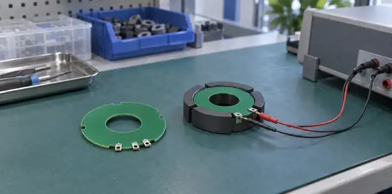
Define the bare-board connections in the fabrication netlist. Identify assembly-completed connections separately. The winding-board electrical-test discussion supports that shipment boundary.
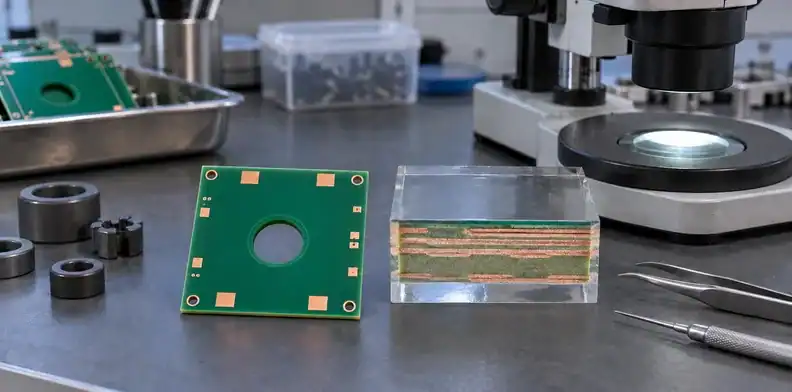
Use a board-construction section review where representative layer or plated-feature evidence is required. Record the sampled location and relate it to the critical winding features. A section taken elsewhere on the board may not describe every feature being approved.
Dimensional acceptance should cover the thickness region and openings used in the core fit review. Report separately supplied window-stack pieces against their own specified dimensions. Keep the board drawing and the reported dimensions traceable to the specimen supplied for assembly.
Core-installed checks follow the operating circuit
Specify the core, mating arrangement, gap where applicable, retention method and insulating materials used in the magnetic trial. Match the measurements to the approved winding diagram and the operating circuit.
Set limits and procedures through the component and product requirements. Loaded thermal behaviour depends on the waveform, losses, mounting and cooling conditions. An unloaded inductance measurement or a bare-board continuity report answers a narrower question.
Record which specimens undergo exposure and which characteristics are checked afterwards. A result for one winding stack and core arrangement should trigger an applicability review before it is reused for a changed construction.
Order the winding PCB with a controlled assembly boundary
Specify whether the order covers a bare winding board, boards with terminals, a core-installed magnetic assembly or a fully qualified component. These scopes require different parts and records even when the fabrication files begin with the same copper patterns.
Provide the winding diagram, layer map, approved stack and core drawings as one controlled package. Include terminal details, insulating pieces and the installation arrangement. Mark unresolved magnetic or insulation assumptions as provisional so the quotation identifies the review still required.
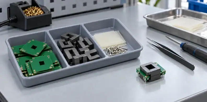
List production boards separately from pilot assemblies and specimens consumed by inspection or qualification. Confirm who supplies the core and retention materials, who installs them and who accepts the magnetic component. Any QueenEMS assembly or test scope should be confirmed for the project.
Review alternatives as complete construction changes. A different core mating piece, dielectric, terminal or winding-board arrangement may affect several interfaces. Ask the proposal to identify the changed geometry and the evidence that needs renewal.
Send the winding diagram, layer-to-net map, core-window drawing, finished-stack requirements and requested assembly boundary through the QueenEMS planar winding-board inquiry. Request separate pricing and stated assumptions for board fabrication, magnetic assembly and any agreed validation work.
Sources
Written by the QueenEMS Engineering Team
Upload your files today · Free DFM check before production · Ship worldwide
Get your PCB prototypes in as fast as 24 hours. We handle FR4, Rogers, and hybrid boards up to 40 layers in volume production, with advanced builds subject to engineering review — free prototypes for 2–4 layer FR-4 boards, no minimum order.
Just upload your Gerber + BOM — we source every part, assemble, and inspect (AOI + X‑Ray) so you don't have to chase suppliers. Boards ship in as fast as 24 hours.