
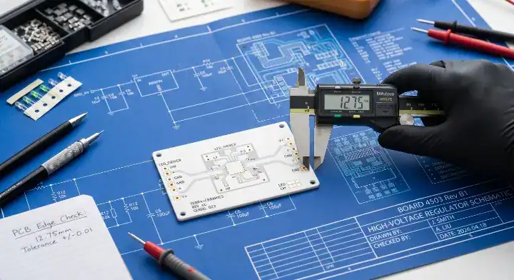
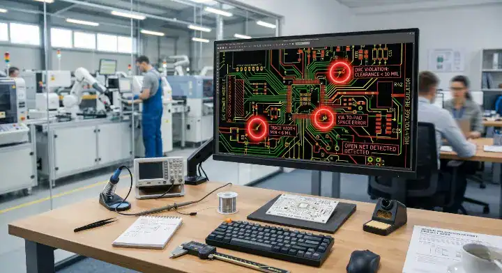
Ceramic PCB Design Rules: 12 DFM Specs Every Engineer Must Know Before Layout directly govern whether your substrate survives manufacturing or cracks during the extreme heat of the sintering oven. When working with a specialized ceramic PCB manufacturer, engineering teams must abandon standard FR4 layout habits and adopt strict guidelines for laser-drilled vias, heavy copper etching, and CTE matching to prevent massive tooling fee losses.
Quick Answer: Designing for ceramic PCBs requires strictly replacing FR4 metrics with specialized rules: minimum trace widths expand to 100–200μm for DBC copper, via diameters drop to 75μm using laser drilling, and double-sided stack-ups demand 100% symmetry to prevent warpage. Feature-to-feature spacing must strictly equal or exceed the board thickness (typically 0.38mm to 1.0mm) to prevent thermal-mechanical cracking.
Key takeaways:
- Brittle Substrates: Alumina and AlN cannot be routed or drilled mechanically; all vias rely on 5:1 aspect ratio laser processing.
- Copper Limits: Thin-film DPC achieves microscopic 25μm traces, while heavy-copper DBC requires wider 150μm clearances due to severe etching undercut.
- Warpage Prevention: Double-sided layouts must maintain copper thickness symmetry within a 20% tolerance to survive high-temperature reflow.
- Edge Clearances: A mandatory 0.5mm to 1.0mm edge margin stops laser-dicing micro-cracks from destroying outer circuit traces.
Table of Contents
- What Makes Ceramic PCB Design Rules Different from FR4?
- Why Are Minimum Trace Widths Different on Ceramic?
- What Are the Ceramic PCB Spacing and Clearance Rules?
- How Do You Design Vias on Brittle Ceramic?
- What Are the Rules for Ceramic PCB Edge Clearance?
- How to Avoid Warpage and Cracking During Reflow?
- What Are the Most Common Ceramic PCB Design Mistakes?
- How Do Different Layer Counts Affect Ceramic Layout?
- What Are the Ceramic PCB Reliability Considerations?
- How to Validate Your Ceramic PCB Design Before Fabrication?
1. What Makes Ceramic PCB Design Rules Different from FR4?
Ceramic PCB design rules differ fundamentally from FR4 because materials like Al2O3 and AlN are extremely brittle, require high-energy laser drilling instead of mechanical bits, and undergo high-temperature sintering that causes massive thermal shrinkage. Treating a ceramic layout like a standard fiberglass board guarantees fractured substrates and lifted pads during manufacturing.
Standard FR4 relies on pliable epoxy resins and glass fibers that forgive aggressive mechanical routing and asymmetric copper pours. Ceramic blanks, however, behave like glass. Mechanical drills will shatter the board immediately. The physical reality dictates that every via must be burned through with a laser, and every panel must be diced using specialized diamond saws. Furthermore, the extreme heat required to bond copper directly to ceramic (often exceeding 1,000°C) means the entire board expands and contracts violently during fabrication.
| Design Parameter | FR4 Standard Rule | Ceramic Standard Rule | Reason for Difference |
|---|---|---|---|
| Via Drilling | Mechanical (0.2mm+) | Laser strictly (0.075mm+) | Mechanical bits shatter the brittle ceramic base. |
| Copper Balance | Flexible / Asymmetric | Strictly 100% Symmetrical | Asymmetry causes severe board warpage during high-heat sintering. |
| Edge Routing | V-score / Route | Diamond saw / Laser score | Ceramic chips and fractures under standard router bits. |
| Trace Undercut | Low (0.5oz–1oz) | Very High (up to 800μm Cu) | Thick copper requires longer etching, widening the required spacing. |
Key Takeaway
- Ceramic requires laser drilling, not mechanical bits.
- Copper symmetry is non-negotiable for preventing warpage.
- Sintering temperatures demand exact thermal expansion planning. Bottom line: Discard your standard FR4 DRC profiles immediately and configure your CAD tool strictly for brittle substrate physics.
2. Why Are Minimum Trace Widths Different on Ceramic?
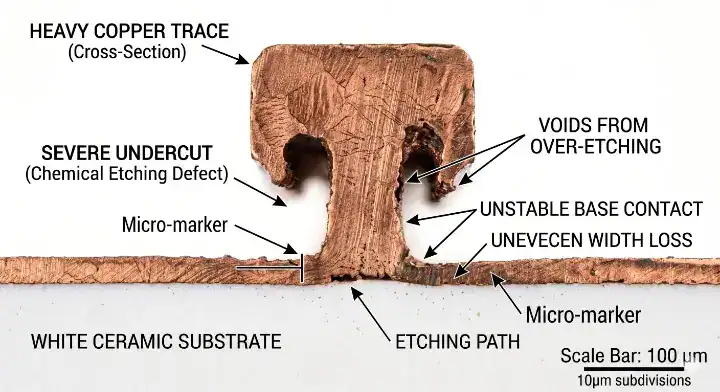
Minimum trace widths on ceramic PCBs range from a microscopic 25μm using thin-film DPC to a massive 200μm using heavy-copper DBC, driven entirely by the aggressive etching undercut caused by bonding thick copper to a flat ceramic base. The fabrication method dictates your trace limits, not the material itself.
Engineers frequently visit the r/PrintedCircuitBoard subreddit with this exact frustration: “Why does my ceramic PCB fab quote a 100μm minimum trace when I can do 75μm on FR4?” The answer relates directly to copper volume. DBC (Direct Bonded Copper) utilizes copper thicknesses between 127μm and 500μm to carry massive automotive or industrial currents. Etching through 500μm of solid copper creates a lateral undercut 5 to 10 times larger than standard 1oz (35μm) FR4. If you attempt a 75μm trace on a DBC board, the etching chemical will dissolve the entire trace away. For tight layouts, you must specify the DPC (Direct Plated Copper) method, which plates very thin copper and achieves 25–50μm traces. Having the ceramic PCB manufacturing process explained clarifies which method fits your footprint.
| Manufacturing Process | Copper Thickness | Min Trace Width | Min Trace Space | Best Application |
|---|---|---|---|---|
| DPC (Thin Film) | 2μm – 105μm | 25μm – 50μm | 25μm – 50μm | High-density RF, LED |
| Thick Film | 10μm – 20μm | 100μm | 100μm | Sensor elements, resistors |
| DBC (Direct Bond) | 127μm – 500μm | 100μm – 200μm | 100μm – 200μm | High-power IGBTs |
| AMB (Active Braze) | 300μm – 800μm | 200μm+ | 250μm+ | EV Traction Inverters |
Key Takeaway
- DBC undercut destroys fine traces during chemical etching.
- DPC supports 25μm traces but costs significantly more.
- Thick film printing bottoms out at a physical 100μm limit. Bottom line: If your design requires high-density routing, select DPC; if it requires massive current capacity, you must accept the 150μm+ spacing rules of DBC.
3. What Are the Ceramic PCB Spacing and Clearance Rules?
Feature-to-feature spacing on a ceramic PCB must be at least equal to the board thickness (typically 0.38mm to 1.0mm) to prevent micro-crack propagation during high-voltage operation and rapid thermal cycling. Placing pads or vias too close together compromises the structural integrity of the brittle base material.
When routing high-power substrates, engineers must balance mechanical spacing against electrical isolation. The critical standard here comes from the IPC-2221 guidelines on trace spacing, which outlines clearance based on voltage withstand requirements. On a ceramic board, the physical mechanical rule often overrides the electrical rule. If you use a 0.635mm thick Al2O3 board, your via-to-via or pad-to-pad minimum spacing should strictly remain at or above 0.635mm. Pushing features closer creates localized stress points that fracture during the 260°C reflow oven cycle.
| Feature Clearance | Minimum Rule | Ideal Safety Margin | Consequence of Violation |
|---|---|---|---|
| Via to Via Pitch | ≥ 1× Board Thickness | 2× Board Thickness | Micro-cracks between vias |
| Pad to Pad (DBC) | ≥ 0.20mm | 0.30mm | Solder bridging, Etch failure |
| Trace to Hole | ≥ 0.30mm | 0.50mm | Hole plating short circuits |
| Component to Edge | ≥ 0.50mm | 1.00mm | Component damage during dicing |
Key Takeaway
- Mechanical spacing rules override electrical clearance charts on ceramics.
- Feature pitch must scale linearly with the board’s physical thickness.
- Tight clustering of features creates dangerous physical stress concentrators. Bottom line: Always set your CAD clearance rules to match or exceed the physical thickness of your ceramic substrate.
4. How Do You Design Vias on Brittle Ceramic?
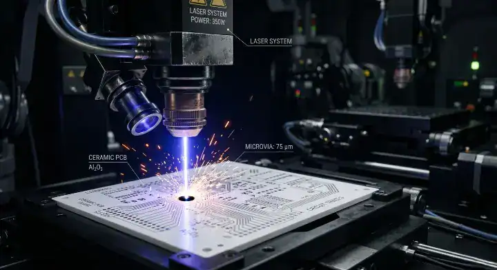
Designing vias on brittle ceramic requires strict laser drilling with a minimum diameter of 75μm and an aspect ratio limit of 5:1 to prevent mechanical chipping and guarantee uniform copper plating inside the via barrel.
A frequent question on the EEVblog forum highlights this physical constraint: “Trying to put thermal vias under a power QFN on alumina — is via-in-pad even possible? Will the ceramic crack?” Yes, via-in-pad is standard, but you must respect the material limits. Mechanical bits will instantly chip the ceramic, so all holes demand laser processing. Because a laser forms a slight V-shape as it burns through the substrate, pushing past a 5:1 aspect ratio prevents copper from plating the center of the hole. Furthermore, if you place via-in-pad arrays under a QFN or BGA, you must mandate copper filling and surface planarization. Without planarization, trapped air inside the via expands during reflow, blowing the solder joint off the board.
A medical device customer came to us in early 2026 with an ultrasonic transducer driver board on AlN substrate. Their design featured 36 thermal vias under a SiC MOSFET, each at 100μm diameter with a tight 200μm pitch. On a 0.38mm thick AlN board, this aspect ratio (~3.8:1) worked for the laser, but the via-to-via spacing was severely below the ceramic thickness — guaranteeing micro-crack propagation. We worked with their EE to redesign the array: we increased the pitch to 400μm, reduced the via count to 18, and specified copper-filled vias with planarization for the MOSFET pad. Thermal simulations showed the effective junction-to-case Rth changed from 0.42 K/W to 0.46 K/W — a negligible 9.5% degradation. After fabrication, 100% of the 240 prototype boards passed thermal cycling (-40°C to +125°C, 500 cycles) with zero crack initiation.
| Via Parameter | Specification Limit | Production Consequence if Broken |
|---|---|---|
| Laser Via Diameter | 75μm (Min) – 150μm (Typical) | Laser cannot focus cleanly below 75μm. |
| Aspect Ratio (Depth:Width) | 5:1 (Maximum) | Copper plating fails to coat the deep center. |
| Via to Edge Distance | ≥ 1× Board Thickness | The edge chips and breaks during laser dicing. |
| Via-in-Pad Requirement | Fill + Planarization Mandatory | Solder voids and component lift-off. |
Key Takeaway
- Laser drilling limits aspect ratios to a strict 5:1 maximum.
- Via-in-pad designs must include copper filling and planarization.
- Excessive via density causes cracking; spacing matters more than quantity. Bottom line: Reduce your total thermal via count and increase the pitch; a well-spaced array prevents the substrate from shattering under thermal stress.
5. What Are the Rules for Ceramic PCB Edge Clearance?
Ceramic PCB edge clearance must be maintained between 0.5mm and 1.0mm to protect delicate outer traces from the mechanical stress and physical chipping caused by laser scoring or diamond-saw dicing during panel separation.
When a factory separates a 4×4 ceramic panel into individual boards, they use a high-speed diamond saw or a pulsed laser. Both methods generate intense localized vibration and heat. If a copper trace sits 0.1mm from the board edge, the dicing process will likely peel the copper back or create a hairline fracture that severs the circuit. Additionally, corners should never be perfect 90-degree angles; applying a minimum radius of R≥0.2mm dissipates handling stress and prevents corner snapping during assembly.
| Routing Rule | Specification | Design Purpose |
|---|---|---|
| Trace to Edge Clearance | 0.5mm – 1.0mm | Prevents copper peeling during dicing. |
| Corner Radius (Fillet) | R ≥ 0.2mm | Eliminates sharp stress concentration points. |
| Saw Street Width | ≥ 0.25mm (10 mil) | Allows physical clearance for diamond saw blades. |
| Breakaway Tabs | Laser scored strictly | Prevents mechanical snapping damage. |
Key Takeaway
- Diamond saws and lasers cause edge micro-fractures during separation.
- A 0.5mm minimum keep-out zone protects outer circuitry.
- Rounded corners significantly reduce mechanical stress concentrations. Bottom line: Keep all active copper and components at least 0.5mm away from the board outline to survive the panel separation process.
6. How to Avoid Warpage and Cracking During Reflow?
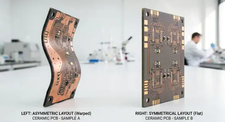
To avoid warpage during reflow, double-sided ceramic PCBs must feature a completely symmetrical stack-up where top and bottom copper thicknesses differ by no more than 20%, ensuring uniform thermal expansion across the brittle base.
Engineers on the All About Circuits forum regularly face this exact disaster: “My double-sided ceramic PCB warped during reflow — what design rule did I break?” The answer is almost always asymmetric copper weight. When a board runs through a 260°C reflow oven, copper expands significantly faster than the ceramic base. If the top layer holds massive 500μm thick copper planes and the bottom layer has only sparse 50μm signal traces, the top layer will violently pull the ceramic upward, bending the board like a potato chip. Furthermore, the board thickness vs size ratio must stay below 1:50; for example, a thin 0.5mm board should not exceed 25mm in total length without high risk of cracking. Finally, the reflow ramp rate must remain extremely gentle, strictly at or below 3°C per second.
| Design Check | Requirement | Result of Violation |
|---|---|---|
| Stack-up Symmetry | < 20% variance top to bottom | Severe board warpage (potato chipping). |
| Thickness to Length Ratio | 1:50 maximum | Mechanical snapping under its own weight. |
| Reflow Ramp Rate | ≤ 3°C per second | Thermal shock shattering the substrate. |
Key Takeaway
- Symmetrical copper layouts prevent uneven thermal expansion.
- Large, thin ceramic boards crack under their own mechanical leverage.
- Rapid temperature changes induce fatal thermal shock. Bottom line: Mirror your top and bottom copper weights exactly; you must balance the thermal pulling forces to keep the ceramic flat.
7. What Are the Most Common Ceramic PCB Design Mistakes?
The most frequent ceramic PCB design mistake is directly copying standard FR4 trace widths, which accounts for 32% of all factory respins and completely ignores the unique heavy-copper etching limits inherent to DBC substrates.
Over the past 18 months, our engineering team has logged the specific design issues we catch during our free DFM reviews on customer ceramic PCB submissions. The top three errors account for 71% of all design respins. First (32%): Minimum trace widths copied from FR4 design rules. Engineers specify a 75μm trace expecting it to work on 300μm DBC copper, and are shocked when we quote a 150μm minimum. Second (24%): Asymmetric stack-ups on double-sided boards. They place 8oz copper on the top layer and 1oz on the bottom, then wonder why the board warps 0.4mm during sintering. Third (15%): Vias placed within 0.3mm of the board edge. Laser drilling executes fine, but the very next thermal cycle propagates a micro-crack straight from the edge to the via hole. We catch all three errors before tooling, but the design rework inevitably adds 5–7 days to the lead time. Reviewing a ceramic PCB price breakdown helps clarify how NRE fees spike when designs require heavy factory modifications.
| Common Mistake | Root Cause | The DFM Fix |
|---|---|---|
| 75μm trace on DBC copper | Ignoring etching undercut | Widen traces to 150μm+ based on copper weight. |
| Asymmetric layer stacks | FR4 layout habits | Balance copper density top and bottom. |
| Vias too close to edge | Tight footprint packaging | Move all vias 1× board thickness away from the edge. |
| Mechanical drill files | Not setting laser rules | Specify laser processing for all holes < 0.2mm. |
Key Takeaway
- Copying FR4 DRC profiles guarantees a factory rejection.
- Unbalanced copper pours cause irreversible warpage.
- Edge-adjacent vias create immediate thermal cracking hazards. Bottom line: Never submit a ceramic design without running a dedicated DFM check specifically configured for DBC or DPC manufacturing rules.
8. How Do Different Layer Counts Affect Ceramic Layout?
Scaling from a single-layer to a multi-layer ceramic PCB exponentially increases layout difficulty, requiring precise step-routing and severely limiting maximum board dimensions to manage the unpredictable firing shrinkage across multiple sintered layers.
While standard FR4 easily stacks up to 60 layers, ceramic boards fight physics at every step. Single-layer boards are cheap, flat, and highly reliable. Double-layer boards introduce the warpage and via-alignment challenges discussed earlier. Multi-layer ceramic boards (like HTCC or LTCC formats) are manufactured by stacking raw, flexible “green tape” ceramics and firing them together. This process shrinks the board by up to 15% in the oven. Designing for this shrinkage requires immense precision, massive tolerances, and strictly limits the overall panel size to prevent layer misalignment.
| Layer Count | Relative Difficulty | Max Practical Size | Primary Layout Challenge |
|---|---|---|---|
| Single Layer | Low | 100mm × 100mm | Managing trace etching undercut. |
| Double Layer | Medium | 80mm × 80mm | Stack-up symmetry and laser via alignment. |
| Multi-Layer (3+) | Very High | 50mm × 50mm | Predicting X/Y axis shrinkage during firing. |
Key Takeaway
- Single-layer ceramic is highly stable and cost-effective.
- Double-layer requires perfect copper symmetry.
- Multi-layer ceramics suffer from up to 15% shrinkage during firing. Bottom line: Keep your ceramic layouts to one or two layers; offload complex logic routing to a secondary FR4 daughterboard.
9. What Are the Ceramic PCB Reliability Considerations?
Ceramic PCB reliability hinges on managing the thermal mechanical stress between the heavy copper layers and the brittle substrate, requiring strict adherence to minimum feature spacing to survive 1,000+ thermal cycles without solder joint fatigue or pad delamination.
Data compiled by industry analysts at Electronic Design confirms that ceramic substrate reliability in power modules depends heavily on the surface finish applied over the copper. Bare copper oxidizes instantly at high temperatures. To protect the traces and prepare them for heavy wire bonding or BGA soldering, specific surface finishes are required. Electroless Nickel Immersion Gold (ENIG) stands as the absolute industry standard for ceramics, providing a perfectly flat surface for via-in-pad components and excellent oxidation resistance up to high temperatures. OSP is rarely used because it degrades rapidly under the thermal profiles required for heavy-copper soldering.
| Surface Finish | Compatibility with Ceramic | Primary Reliability Benefit |
|---|---|---|
| ENIG (Gold) | Excellent (Industry Standard) | Perfectly flat for BGA, excellent wire bonding. |
| Immersion Silver | Good | High conductivity, cost-effective for LED. |
| ENEPIG | Premium | Ultimate wire bonding reliability (Gold/Aluminum wire). |
| OSP | Poor | Degrades under high-temperature assembly profiles. |
Key Takeaway
- Thermal mechanical stress is the primary enemy of ceramic reliability.
- Surface finish dictates assembly yield and wire-bonding success.
- ENIG and ENEPIG are the mandatory finishes for high-reliability modules. Bottom line: Always specify an ENIG or ENEPIG surface finish to guarantee flat, oxidation-free pads for high-temperature soldering and wire bonding.
10. How to Validate Your Ceramic PCB Design Before Fabrication?
Validating your ceramic PCB design requires cross-referencing your Gerber files against the IPC-6012 Class 3 standard for rigid substrates and running a complete Design for Manufacturability (DFM) check before tooling to eliminate hidden physical violations.
The governing rules for quality inspection sit within the IPC-6012 standard for rigid PCBs, which dictates exact requirements for annular rings, plating thickness, and defect tolerances. Before you send your files to a factory, learning how to order your first ceramic PCB prototype helps align your Gerber output with factory expectations. Use the following 12-point cheatsheet to execute a final self-audit.
| The 12-Point Ceramic DFM Cheatsheet | Required Spec |
|---|---|
| 1. DPC Min Trace/Space | 25μm – 50μm |
| 2. DBC Min Trace/Space | 100μm – 200μm |
| 3. Minimum Via Diameter | 75μm (Laser strictly) |
| 4. Max Via Aspect Ratio | 5:1 |
| 5. Board Edge Clearance | 0.5mm – 1.0mm |
| 6. Corner Fillet Radius | R ≥ 0.2mm |
| 7. Saw Street Width | ≥ 0.25mm |
| 8. Feature-to-Feature Spacing | ≥ Board Thickness |
| 9. Standard Board Thickness | 0.25mm to 2.0mm |
| 10. Fabrication Tolerance | ±50μm |
| 11. Copper Thickness Options | 2μm (DPC) up to 800μm (AMB) |
| 12. Double-Sided Stack-up | 100% Symmetrical Cu Weight |
Key Takeaway
- IPC-6012 dictates the global quality standards for ceramic fabrication.
- A 12-point manual review catches the errors CAD software misses.
- Passing a strict DFM checklist prevents expensive tooling respins. Bottom line: Keep this 12-point cheatsheet pinned next to your workstation and verify every metric before exporting your final Gerber files.
Wrapping Up
Designing a ceramic PCB correctly the first time requires accepting the rigid physics of alumina, aluminum nitride, and silicon nitride. By enforcing strict 5:1 via aspect ratios, acknowledging the massive etching undercut of heavy DBC copper, and maintaining perfect symmetry on double-sided layouts, you eliminate the mechanical stresses that fracture substrates during production.
At QueenEMS, our engineering team catches critical layout errors daily before they hit the manufacturing floor. We analyze your trace clearances, via densities, and thermal stress points against actual factory capabilities. Sending your design through our free PCB DFM check guarantees your board will survive both the sintering oven and your final high-power application.
Ready to lock in your design and move to prototyping? Reach out and contact us today to review your Gerber files with our ceramic fabrication experts.
Written by the QueenEMS Engineering Team
Upload your files today · Free DFM check before production · Ship worldwide
Get your PCB prototypes in as fast as 24 hours. We handle FR4, Rogers, and Flex up to 60 layers — free prototypes for 2–4 layer boards, no minimum order.
Just upload your Gerber + BOM — we source every part, assemble, and inspect (AOI + X‑Ray) so you don't have to chase suppliers. Boards ship in as fast as 24 hours.