
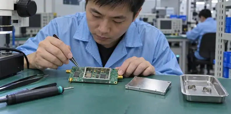
Quick Answer: RF shielding PCB design means specifying the can and its connection to the board as one assembly. Choose a soldered can, removable lid or clip-mounted cover around the required access, then review the ground reference, exact footprint, signal crossings and mechanical clearances. Confirm the result on the populated board under the operating conditions that caused the interference.
A shield can may fit the board outline and still obstruct inspection, leave a signal crossing poorly referenced or interfere with a tall component. These problems begin at different interfaces, so a drawing marked “RF shield” gives the assembler too little information.
The useful starting point is the proposed component and the circuit it surrounds. This guide follows those interfaces through layout, assembly and validation so the released PCB files describe a shield that can be built, serviced and evaluated.
Table of Contents
- Find the interference path before choosing a shield
- Choose a can that permits the required access
- Make the PCB part of the shield boundary
- Review the exact land pattern and clip drawing
- Plan every signal crossing through the boundary
- Check internal height, apertures and temperature
- Schedule assembly around cleaning and inspection
- Separate joint inspection from shielding evidence
- Compare the real assembly with and without the shield
- Release a complete shield interface for quotation
Find the interference path before choosing a shield
RF shielding PCB layout starts by locating the source, victim and coupling path before adding a metal can. Record which circuit changes behavior, the unwanted frequencies and the operating state that exposes the problem. An emission near a receiver is a different starting condition from noise arriving through that receiver’s power connection.
Harwin’s shielding guide distinguishes radiated interference from interference carried along conductors. Determine how surrounding the circuit with conductive material would interrupt the suspected path before specifying the enclosure.
Try a controlled diagnostic change where it is safe to do so. Keep the supply, firmware mode, cable placement and measurement setup constant while changing the local shield configuration. Record whether the unwanted tone or receiver error changes. A temporary cover can help locate a coupling path, but its fit and attachment do not qualify a production shield.
For example, a receiver that loses sensitivity only while a neighboring converter operates needs both an operating-mode record and a spectrum comparison. If the disturbance remains after local shielding, inspect the supply and interconnect paths before enlarging the can. If it falls, use the result to identify which region deserves a production enclosure.
Keep antenna behavior in the review. Metal near an antenna can alter its environment even when it helps another circuit. The antenna layout and manufacturing review belongs alongside the shield outline when both share a small board.
Choose a can that permits the required access
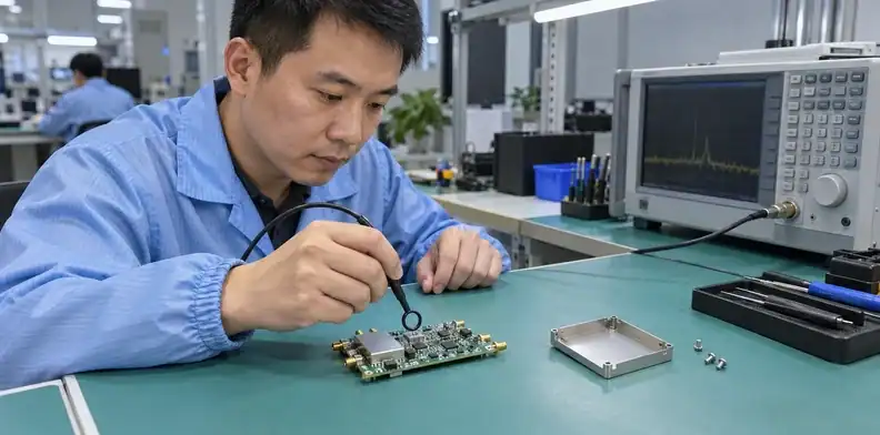
Select the attachment style around inspection, tuning and service access. The decision should include how the assembly will be opened and who must reach the components inside.
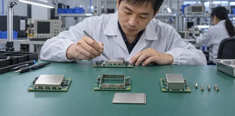
Laird’s board-level shield description separates a soldered one-piece enclosure from a two-piece frame with a removable cover. Its access distinction matters when test points or components sit inside the perimeter.
| Shield arrangement | What remains on the PCB | Access decision before layout | Detail to release |
|---|---|---|---|
| One-piece soldered can | The whole can after soldering | Can inspection and adjustment finish before closure? | Complete can drawing and attachment footprint |
| Soldered frame with lid | Frame stays while lid is removed | Can tools reach past the frame wall? | Matched frame/lid part numbers and installation method |
| Clip-mounted can | Soldered clips retain a separate cover | Is removal permitted during test or service? | Compatible can-wall thickness and clip positions |
| Custom compartmented shield | Defined walls and contacts | Which compartments need independent access? | Full mechanical drawing and partition interface |
A removable lid creates access above the circuit; the surrounding wall still limits sideways tool movement. Check probe tips, rework nozzles and connector latches in the open configuration. A component placed beside the frame may remain difficult to replace.
Keep matched parts together in the BOM. A cover from another family may look compatible while having different contact features or engagement geometry. Purchasing should treat the frame, lid and clips as a documented combination. Any proposed substitution needs a comparison of the attachment interface and the planned RF test, as well as its outside dimensions.
Make the PCB part of the shield boundary
A board-level shield needs a defined PCB reference and a deliberate connection around its perimeter. The metal above the components is only part of the enclosure.
Identify the bottom reference and return
The InCompliance discussion of PCB-level shielding describes the board side, seams and penetrations as parts of the shielding boundary. Apply that perspective to the layer stack: identify the reference beneath the enclosed circuit, the net assigned to the attachment lands and the connections between them.
Inspect the actual copper connectivity. A ground label on a schematic does not show whether the shield lands connect through a narrow neck, an isolated pour or a suitable reference structure. Use the distinction between a copper pour and a ground plane to review that relationship in the released board data.
Perimeter connections must suit the circuit and frequency range. Establish their geometry through the RF layout or electromagnetic review; a DC continuity result alone leaves their RF behavior unresolved. Avoid copying a single via spacing from an unrelated module without its stackup and operating conditions.
Keep the shield perimeter distinct from board-edge plating
A can around an internal circuit and plating on the routed board outline are separate structures. They can cooperate in a design, but their drawings control different surfaces and processes.
For a design that also requires conductive board edges, keep the plated-edge requirements in their own fabrication notes. The can interface still needs its component footprint, wall envelope and installation details. Approving the plated outline does not approve the removable cover.

Review the exact land pattern and clip drawing
Use the selected component drawing to separate mechanical engagement from copper, mask and paste geometry. Importing a generic rectangular shield footprint can miss the feature that actually retains the part.
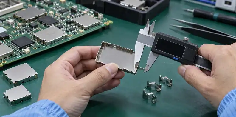
Consider this illustrative drawing review. Harwin S1711-46R specifies compatibility with removable cans having wall thickness from 0.17 to 0.30 mm. A proposed 0.15 mm can is outside that published range. Select a supported combination or obtain explicit component-manufacturer approval before releasing the substitution. A hand-fitted sample alone does not extend the stated range.
| Review item | Evidence to compare | Decision produced |
|---|---|---|
| Clip engagement | Can-wall thickness versus clip specification | Supported combination or approval request |
| Copper lands | Exact MPN land pattern and board revision | Correct electrical and soldering locations |
| Mask openings | Pad geometry and agreed registration allowance | Exposed attachment lands without unintended copper exposure |
| Paste apertures | Component guidance and assembly process review | Controlled deposits for the actual joints |
| Height definition | Above-board dimensions and assembled cover geometry | Check against neighboring parts and enclosure |
The same product page states a maximum above-PCB height of 3.55 mm. That is a clip dimension, so review it separately from the cover’s internal clearance and outside height. Adding or equating unrelated height dimensions can produce an incorrect assembly envelope.
Use the pad-specific solder-mask opening review when defining exposed attachment copper. Paste belongs in its own manufacturing layer. An exposed ring does not automatically require a continuous paste deposit around the entire can. The assembler should review the proposed deposit pattern with the chosen part and process.
Plan every signal crossing through the boundary
Treat each signal crossing as an electrical transition and a mechanical clearance problem. List the nets entering the shielded region, their layers and their associated returns before routing under a wall or through an opening.
Preserve the return at an RF crossing
An inner-layer trace may pass beneath the attachment lands, but its reference must remain suitable through that transition. Review plane interruptions, vias and nearby wall connections together. Where a routed signal requires controlled impedance, keep its approved impedance geometry and reference requirements attached to the shield review.
Power and low-frequency control lines may require different treatment from the RF port. Put any necessary filtering in a deliberate relationship to the boundary so an unfiltered conductor does not simply carry the disturbance through the enclosure. The circuit designer owns that electrical choice; the shield footprint supplies the physical constraints.
Separate wall clearance from routing permission
A Cadence community user question describes package-spacing errors for components placed inside a shield. This is a real CAD representation problem: the volume under the lid is different from the solid wall volume.
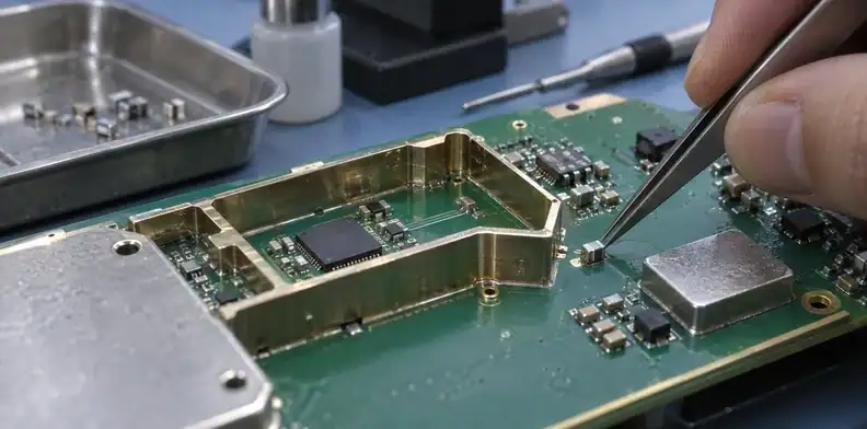
Build the component envelope so the CAD check can distinguish those regions. Verify minimum ceiling height, wall thickness and outside envelope using the chosen tool’s supported properties. Keep clearance rules for the wall and rework access active. Disabling a whole package-spacing check can hide a real collision while eliminating the unwanted warnings.
Check internal height, apertures and temperature
Approve the assembled interior, exterior and openings as one mechanical envelope. Nominal lid height is insufficient when the tallest enclosed component has a package tolerance, solder standoff and local board deformation.
| Envelope feature | Review against | Reason to hold approval |
|---|---|---|
| Lid interior | Maximum assembled component envelope | Potential contact or inadequate clearance |
| Wall and clips | Parts, traces, connector access and tooling | Collision or inaccessible repair location |
| External height | Housing, adjacent board and mounting hardware | Product enclosure does not close correctly |
| Ventilation or access holes | Interference spectrum and thermal comparison | Proposed opening lacks validation |
| Thermal contact to cover | Intended material, pressure and electrical isolation | Unspecified contact changes the assembly |
Openings affect the enclosure and need evaluation at the relevant interference frequencies, including significant harmonics. Avoid approving a hole solely from the circuit’s nominal carrier frequency. A supplier’s material shielding figure also does not describe the behavior of the finished enclosure with its seams, apertures and board connections.
The full lid can change airflow and component temperature. Compare the thermal state under the same power and enclosure conditions used for the RF evaluation. For a power amplifier, retain its separate CW heat-load and cooling-boundary analysis.
A replacement cover that is taller may clear an inductor but changes the cavity geometry. Treat that as a design change with a mechanical benefit and a fresh RF verification requirement. Do not transfer the old result solely because the attachment perimeter stayed the same.
Schedule assembly around cleaning and inspection
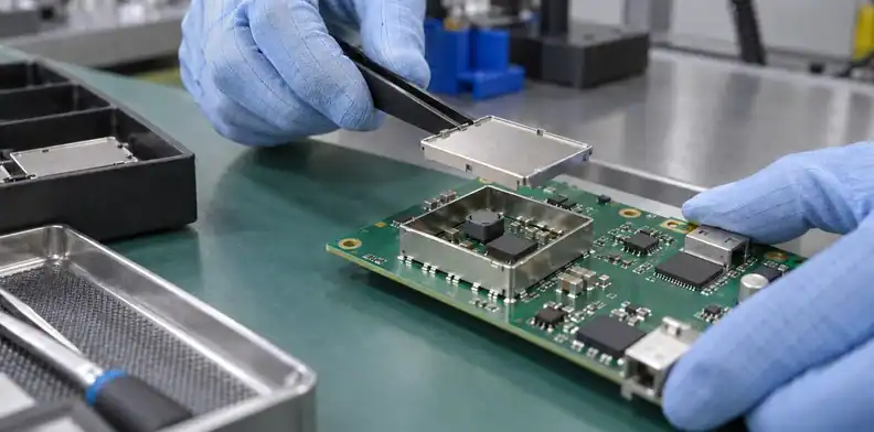
Place lid installation at a defined point in the assembly route, after the checks that require open access. The route must identify which parts pass through soldering and which are installed afterward.
Inspect the populated board before fitting the lid
For a removable configuration, plan the inspection of enclosed joints while they are visible. Specify any electrical adjustments or probe measurements that require the open frame. Then perform the final checks appropriate to the closed assembly.
Cleaning access deserves the same attention. The process engineer should review whether the geometry traps residues or blocks the chosen cleaning and drying route. Use the scope of ionic-cleanliness evidence to define what a report covers. A bare-board cleanliness record does not describe residues introduced by later assembly.
In an illustrative production sequence, the clips are soldered with the board, the accessible joints are inspected, the agreed cleaning process is completed, and the can is fitted before final functional verification. Actual ordering depends on the selected parts and process; write it into the traveler instead of leaving installation to informal bench practice.
Specify removal and reinstallation during rework
Name the permitted removal method and any replacement requirement. Check whether the component manufacturer permits reuse, and record damage to the cover or retention features. Leave room for the intended tools before freezing nearby component placement.
After a repair under the cover, repeat the affected inspection and functional checks, then confirm lid seating in the restored configuration. Keep the rework record associated with the assembly serial or lot so later testing can identify which configuration was evaluated.
Separate joint inspection from shielding evidence
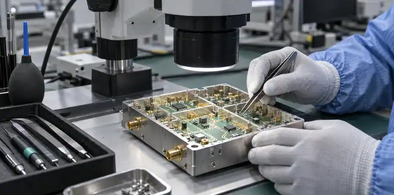
Inspect attachment and fit first, then evaluate RF behavior with a separate electrical test. Each type of evidence answers a different question about the assembly.
| Evidence | Useful finding | Additional work still needed |
|---|---|---|
| Open-frame optical inspection | Visible joint and component placement condition | Verification after closure |
| Clip or frame joint inspection | Attachment workmanship at accessible locations | Cover engagement and RF comparison |
| DC continuity measurement | Intended conductive connection exists at the test points | Behavior over the relevant frequencies |
| Mechanical fit inspection | Lid engagement and absence of visible collision | Thermal and electrical operation |
| RF or susceptibility test | Performance under the recorded setup | Coverage of other required modes and product conditions |
An optical check made before the lid is fitted should be recorded as that stage’s result. It cannot show a later installation error. Likewise, a continuity measurement should identify its probe points and net; “shield grounded” is too vague to interpret when several conductive structures are nearby.
Select the inspection method around the joint and failure mode. The AOI, X-ray and electrical-test comparison helps separate visible workmanship from hidden joints and electrical behavior.
Keep the shield’s part revision in the evidence package. If purchasing changes the frame, cover finish or clip, the receiving record and assembly traveler should identify the replacement. Quality can then determine which inspections and design tests must be repeated instead of accepting an unidentified enclosure under the old approval.
Compare the real assembly with and without the shield
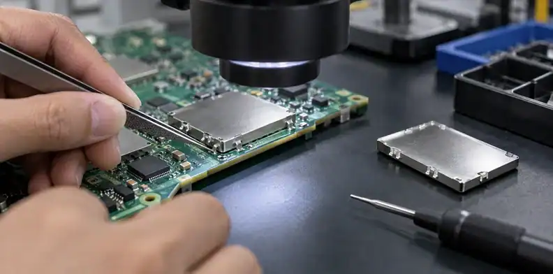
Run a controlled comparison on the proposed assembly over its relevant operating modes. Record the operating state and test geometry closely enough that another engineer can repeat it.
Use the same operating and measurement conditions
XGR’s published shielding analysis describes a fixture comparing received signals with and without a shield and discusses frequency-dependent cavity behavior. Compare the proposed enclosure over the relevant frequency range; its vendor-specific results do not establish attenuation for another board.
On your prototype, fix the source setting, receiver setting, cable routing and probe position. Record lid state and board temperature. For receiver interference, include the affected receiver metric where possible; a lower near-field reading alone may leave the actual functional problem unresolved.
An illustrative review might find that a removable lid reduces one unwanted tone while another persists. Repeat the measurements to check reproducibility, then examine the residual path. This is a proposed diagnostic sequence, with no assumed attenuation or successful outcome.
Explain a disappointing shielding result
A weak result can come from a conductor crossing the boundary, a poor connection, an aperture or a different path outside the shielded region. A narrow frequency peak also warrants investigation of the enclosure and its contacts.
Change one feature at a time where practical, and keep the altered configuration in the test record. Once the root cause is understood, repeat the relevant test on the intended production construction. Product compliance limits, detector settings and operating modes should come from the applicable product test plan; a convenient bench setup does not define them.
Release a complete shield interface for quotation
Provide the shield parts and PCB interface with the intended assembly and verification sequence. This lets the supplier identify unresolved fit or process details before they become production assumptions.
| RFQ input | Include | Responsible approval |
|---|---|---|
| Board data | Gerber or ODB++, net reference and attachment geometry | PCB/layout engineering |
| Shield BOM | Exact can, frame, lid and clip MPNs with approved alternates | Component engineering and purchasing |
| Mechanical assembly | STEP models, maximum height and installation access | Mechanical engineering |
| Assembly route | Soldering parts, cleaning, open inspection and lid-installation stage | Manufacturing engineering |
| Verification scope | Required functional/RF checks, configurations and report contents | Design engineering and quality |
Specify who can approve changed wall thickness, aperture patterns, lid engagement or part substitutions. The assembler can identify a manufacturability issue, but a process suggestion that changes the enclosure needs the relevant design approval.
An RFQ should also explain whether the supplier is assembling a fully specified shield or evaluating alternative constructions. Those are different scopes of work. If the electrical reference, matched parts or final test configuration is still unresolved, close that decision before treating the production quote as released.
For a QueenEMS project, send the board files, shield BOM and assembly drawing with the access and verification requirements. A specific interface package makes the quotation discussion actionable and gives both sides a common revision to review.
Sources
Written by the QueenEMS Engineering Team
Upload your files today · Free DFM check before production · Ship worldwide
Get your PCB prototypes in as fast as 24 hours. We handle FR4, Rogers, and hybrid boards up to 40 layers in volume production, with advanced builds subject to engineering review — free prototypes for 2–4 layer FR-4 boards, no minimum order.
Just upload your Gerber + BOM — we source every part, assemble, and inspect (AOI + X‑Ray) so you don't have to chase suppliers. Boards ship in as fast as 24 hours.