
Quick Answer: When evaluating a 4 layer vs 6 layer pcb stackup,upgrading from a 4-layer to a 6-layer PCB stackup increases mass production costs by 30%–40% and adds 1–2 days to fabrication lead times, but it provides two dedicated solid ground planes for superior signal integrity. You must make this upgrade when routing a BGA with a 0.8mm pitch or when isolating a high-speed 24-bit ADC near a noisy switching regulator.
Key takeaways:
- Prototype cost differences are minor ($30–$80 total), but mass production (1,000+ units) costs jump by 30%–40%.
- Standard 6-layer 1.6mm boards use thinner prepreg (0.1mm–0.2mm), requiring thinner trace widths for 50-ohm impedance control.
- Splitting a ground plane on a 4-layer board is a massive EMI risk; a 6-layer board solves this with solid, continuous reference planes.
- 0.8mm BGA pitch is the physical routing limit where standard 6-layer boards become significantly cheaper than forcing HDI microvias on a 4-layer design.
Table of Contents
- 1. What is the Core Difference Between 4-Layer and 6-Layer PCBs?
- 2. Standard 4-Layer PCB Stackup: What Are The “Signal-GND-Power-Signal” Basics?
- 3. Standard 6-Layer PCB Stackup: Where Do the Extra Layers Go?
- 4. Signal Integrity & EMI: When Does a 4-Layer Board Fail?
- 5. Routing Density: Do You Pass The BGA Pitch Test for 6-Layer Upgrades?
- 6. Cost Analysis: How Much More Will a 6-Layer PCB Cost?
- 7. Manufacturing Lead Time: Do 6-Layer Boards Take Longer?
- 8. Red Flags & Green Flags: How to Use The 4 vs 6 Layer Decision Matrix?
- 9. Need Help Deciding? Why Not Get a Free Stackup DFM Check?
Operating a facility with a 99.7% first-pass yield rate teaches you quickly where hardware teams lose money. Hardware engineers frequently design themselves into a corner by squeezing complex routing into a 4-layer board to save a few dollars, only to fail EMI certification later. Blindly upgrading causes your purchasing manager to reject the BOM due to unexpected cost spikes. This guide will give you the exact technical thresholds to decide exactly when to move forward with a 4 layer vs 6 layer pcb stackup without wasting your budget.
1. What is the Core Difference Between 4-Layer and 6-Layer PCBs?
A standard 4-layer PCB has two external routing layers and two internal planes, while a 6-layer PCB adds two additional internal routing layers or ground planes. This physical upgrade provides a continuous return path for high-speed signals, reducing crosstalk by up to 60% compared to a standard 4-layer configuration.
Return path is the route high-frequency current takes back to its source, typically requiring less than 0.1mm distance to the reference plane for maximum EMI control. When traces cross gaps in planes on a 4-layer board, the return path balloons outwards, creating a massive loop antenna. A 6-layer board fixes this by sandwiching traces tightly between solid reference planes.
Look at the reality of the situation:
- 4-layer boards force compromises between power distribution and signal routing.
- 6-layer boards allow dedicated, unbroken ground planes.
- 6-layer boards enable tighter trace routing due to closer reference planes.
- 4-layer boards are cheaper but carry higher EMI failure risks for mixed-signal designs.
Bottom line: Stick to a 4-layer board for basic digital logic circuits, but immediately upgrade to a 6-layer board when your design requires strict mixed-signal isolation and continuous return paths.
2. Standard 4-Layer PCB Stackup: What Are The “Signal-GND-Power-Signal” Basics?
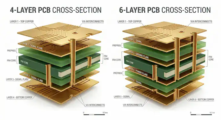
The most common 4-layer PCB stackup places signals on the top and bottom layers, with a solid ground plane on layer 2 and a power plane on layer 3. In a standard 1.6mm total thickness, the core between layer 2 and 3 is typically 1.2mm thick, creating a wide gap that destroys inter-plane capacitance.
Because the core is so thick, high-frequency noise has no natural capacitive dampening between the power and ground planes. Furthermore, if you need to route a 50-ohm single-ended trace on the top layer, the distance to the layer 2 ground plane dictates the trace width.
Here is the catch:
- A standard 4-layer 1.6mm board uses roughly 0.2mm prepreg on the outer layers.
- Traces on layer 1 must reference layer 2 for their return path.
- Traces on layer 4 must reference the power plane on layer 3, which is terrible for signal integrity.
- You can read more about foundational stackup strategies in our 2 Layer vs 4 Layer PCB comparison.
Bottom line: A standard 4-layer stackup is highly cost-effective for simple microcontrollers, but it fails structurally when you need tightly coupled power and ground planes for high-speed decoupling.
3. Standard 6-Layer PCB Stackup: Where Do the Extra Layers Go?
A standard 6-layer PCB stackup standard 1.6mm configuration positions signals on layers 1, 3, 4, and 6, using layers 2 and 5 exclusively as solid ground planes. This arrangement guarantees every single routing layer is directly adjacent to a solid reference ground, separated by only 0.1mm to 0.2mm of prepreg.
When a client recently submitted a 4-layer design that failed FCC testing, we reviewed their gerbers and immediately moved their noisy traces between two solid ground planes on a standard 6-layer stackup. This simple structural change resulted in a 15 dB drop in radiated emissions, and they passed certification the following week.
Consider the structural benefits:
- Layer 2 and Layer 5 act as massive EMI shields for the internal signal layers.
- Power is usually routed as thick traces or copper pours on the internal signal layers (Layer 3 or 4).
- The thin prepreg (0.1mm) between layers 1-2 and 5-6 makes 50-ohm trace widths much narrower and easier to route.
- Blind and buried vias become an option, though they drastically increase costs.
Bottom line: Upgrading to six layers is not just about gaining routing space; it is about physically sandwiching your high-speed traces between solid ground planes to kill electromagnetic radiation.
4. Signal Integrity & EMI: When Does a 4-Layer Board Fail?
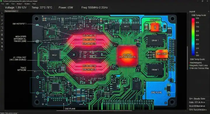
A 4-layer board fails EMI testing when designers try to route a high-speed 24-bit ADC next to a noisy switching regulator by using split ground planes. Adding two extra layers allows you to use a continuous, solid ground plane that blocks switching noise and protects sensitive analog signals from digital interference.
We constantly see hardware teams on forums like Electronics StackExchange asking: “I have a design with a high-speed ADC (24-bit) and a noisy switching regulator. Is a 4-layer board with split planes enough, or must I use 6 layers?” Splitting ground planes on a 4-layer board is extremely dangerous. When a high-speed signal trace inevitably crosses that split in the plane, the return current path is broken. This creates a massive impedance discontinuity and turns your PCB into a broadband radiator. A 6-layer stackup solves this entirely by allowing you to dedicate full, un-split solid ground planes for isolation. You can dive into more configuration details in our PCB Stack-up Design Guide.
Keep these rules in mind:
- Split planes force return currents to take long, noisy detours.
- Unbroken ground planes naturally contain high-frequency magnetic fields.
- 24-bit ADCs require zero ground bounce to function accurately.
- Switching regulators require tight, localized return loops that a 6-layer board provides.
Bottom line: Never split ground planes on a 4-layer board to isolate mixed signals; invest the budget into a 6-layer stackup to maintain a solid, continuous reference plane.
5. Routing Density: Do You Pass The BGA Pitch Test for 6-Layer Upgrades?

You must upgrade to a 6-layer PCB when trying to route a BGA with a 0.8mm pitch or smaller, because a 4-layer board physically lacks the space for proper escape routing. Shrinking traces below 4 mils on a 4-layer board to squeeze between BGA pads increases fabrication failure rates by 15%, making a standard 6-layer board the cheaper and more reliable choice.
Engineers on r/PrintedCircuitBoard frequently ask: “Trying to route a BGA with a 0.8mm pitch on a 4-layer board, running out of space for the inner balls. Should I switch to HDI or just add 2 more standard layers?”
The engineering reality is blunt. For 0.8mm and below pitch BGAs, 4-layer escape routing is a nightmare. You will run out of vias and routing channels on the inner layers. Directing your design to a standard 6-layer stackup gives you two extra routing layers instantly. This is drastically cheaper and much more reliable than forcing costly HDI microvias or via-in-pad technology onto a crowded 4-layer board.
The math is simple:
- 0.8mm pitch leaves roughly 0.4mm between pads.
- Standard 4 mil traces and 4 mil spacing require at least 0.3mm of clearance.
- 4-layer boards limit you to essentially two effective escape layers.
- 6-layer boards provide the inner layers needed to fan out the center BGA balls safely.
Bottom line: Treat a 0.8mm BGA pitch as your hard limit—once you hit this threshold, stop struggling and upgrade to a standard 6-layer design rather than paying massive premiums for HDI on 4 layers.
6. Cost Analysis: How Much More Will a 6-Layer PCB Cost?
Upgrading from a 4-layer to a 6-layer board increases prototype (5-10 pcs) costs by only $30 to $80, but mass production (1,000+ units) unit prices jump significantly by 30% to 40%. The 6-layer pcb stackup also adds roughly $150 to $200 in testing costs if you mandate strict 50-ohm controlled impedance reports from the factory.
NRE (Non-Recurring Engineering) fees are one-time charges for tooling and setups. For a standard 6-layer board, NRE typically ranges from $150 to $300, barely higher than a 4-layer board. However, the raw material (FR4 core and prepreg) and the pressing labor add up fast at scale.
Here is the reality of your budget:
| Feature | 4-Layer PCB | 6-Layer PCB |
|---|---|---|
| Number of Routing Layers | 2 (External) | 4 (2 External, 2 Internal) |
| EMI Shielding | Poor to Moderate | Excellent |
| Cost Premium | Baseline | +30% to 40% (at volume) |
| Typical BGA Pitch Limit | 1.0mm | 0.8mm or 0.65mm |
| Best Used For | Simple microcontrollers, IoT nodes | High-speed logic, FPGAs, mixed-signal |
Choose a 4-layer board for prototype iterations where keeping the initial cash burn low is critical. Choose a 6-layer board when moving to mass production if failing an EMI certification would delay your product launch and cost you millions.
| Stackup Type | Prototype NRE Cost | Mass Production Unit Cost (1000+) | Standard Lead Time |
|---|---|---|---|
| Standard 4-Layer | $100 – $150 | $2.00 – $4.00 | 3 – 5 Days |
| Standard 6-Layer | $150 – $200 | $2.80 – $5.60 | 5 – 7 Days |
Because 6-layer boards require more material and machine time, the unit cost scales aggressively as your volume grows.
Bottom line: Do not let a cheap $50 prototype price difference trick you into a 6-layer design if your mass production margins cannot absorb a 40% unit cost increase later.
7. Manufacturing Lead Time: Do 6-Layer Boards Take Longer?

Fabricating a 6-layer PCB adds 1 to 2 full days (24 to 48 hours) to your standard lead time because it physically requires a secondary lamination cycle. While a standard 4-layer board can be pressed once, six layers require pressing the inner core, baking it, and then pressing the outer layers again.
Buyers often demand a 24-hour fastest turnaround for highly complex boards. When a startup recently pushed for next-day delivery on a 6-layer board, we explained the physics of lamination curing times. We agreed on a 3-day turnaround instead, allowing us to perform full 3D AOI and X-Ray inspection on every BGA joint, resulting in a 100% functional batch. Check our PCB Fabrication Lead Time guide for detailed timelines.
Understand the timeline shift:
- For prototype runs (5-10 pcs): expect 3-5 days for 4-layer, and 5-7 days for 6-layer.
- For mid-volume runs (100-500 pcs): expect 7-10 days for 4-layer, and 10-12 days for 6-layer.
- For high-volume mass production (1000+ pcs): expect 2 weeks for 4-layer, and up to 3 weeks for 6-layer.
- Expedited services exist, but curing epoxy resin cannot be magically bypassed.
Bottom line: If your project timeline is absolute and you require a 24-hour turnaround, simplify your design to 4 layers; otherwise, plan for a 3-to-5 day minimum manufacturing cycle for 6 layers.
8. Red Flags & Green Flags: How to Use The 4 vs 6 Layer Decision Matrix?
A major red flag for forcing a 4-layer design is having more than three BGAs with under a 1.0mm pitch, which guarantees routing bottlenecks and manufacturing defects. A green flag for a 6-layer upgrade is the presence of high-speed memory interfaces like DDR4, which strictly require adjacent, solid ground reference planes to function.
Making the wrong choice early in Altium or KiCad guarantees a costly redesign. Use this binary framework to make a fast, correct decision.
Check your design against these flags:
- Red Flag (Avoid 4-layer): You have analog sensors sitting right next to heavy switching power supplies.
- Red Flag (Avoid 4-layer): You are forced to route high-speed traces across a split in your ground plane.
- Green Flag (Choose 6-layer): Your board includes dense FPGAs that require multiple internal routing channels for escape.
- Green Flag (Choose 6-layer): You need strict 50-ohm single-ended and 90-ohm differential impedance control on multiple layers.
Bottom line: Stop wasting engineering hours squeezing traces into a 4-layer board when a 6-layer upgrade pays for itself immediately through faster routing time and guaranteed EMI compliance.
9. Need Help Deciding? Why Not Get a Free Stackup DFM Check?
Guessing on your layer count creates severe financial risks when scaling up to mass production. We offer a Free DFM/DFA engineering review on every order, allowing our experts to analyze your Gerber files and tell you exactly if a 4-layer board is safe, or if a 6-layer board is mandatory.
At QueenEMS, our full turnkey service takes you from component sourcing to final testing without the headaches. With our capability to fabricate up to 60-layer PCBs and perform 3D AOI + X-Ray inspection on every BGA joint, your complex designs are in safe hands. Furthermore, we offer free 2-4 layer FR4 prototypes for new customers to prove our 99.7% first-pass yield rate.
Stop fighting routing bottlenecks on your own. Submit your files to our engineering team today, and let us build a reliable, cost-effective stackup strategy for your next product launch.
Frequently Asked Questions (FAQ)
Can I use a 4-layer board for DDR4 memory? No, you cannot reliably route DDR4 on a 4-layer board. DDR4 requires strict impedance control, extremely tight length matching, and solid adjacent ground planes for return currents, which a 6-layer board provides naturally. If you are designing high-speed memory, contact us for a 6-layer stackup recommendation.
How much thicker is a 6-layer board than a 4-layer board? They are exactly the same thickness if you order a standard 1.6mm board. The manufacturer simply uses thinner internal core and prepreg materials (like 0.1mm thickness) to fit the two extra copper layers into the same overall standard profile. Need a custom thickness? Upload your BOM for a quick quote.
Do 6-layer boards take longer to manufacture? Yes, they typically add 24 to 48 hours to your fabrication lead time. This is because 6-layer boards require two separate lamination pressing and curing cycles in the factory, whereas a 4-layer board only requires one. If you are on a tight deadline, ask our team about our expedited manufacturing options.
Written by the QueenEMS Engineering Team
Upload your files today · Free DFM check before production · Ship worldwide
Get your PCB prototypes in as fast as 24 hours. We handle FR4, Rogers, and Flex up to 60 layers — free prototypes for 2–4 layer boards, no minimum order.
Just upload your Gerber + BOM — we source every part, assemble, and inspect (AOI + X‑Ray) so you don't have to chase suppliers. Boards ship in as fast as 24 hours.