
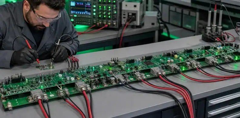
Quick Answer: Large PCB power distribution should be designed from a load-and-return map, not from one trace-width rule. Budget source, connector, fuse, copper, via and return resistance to every distant load; then validate node voltage, local ground shift and temperature across real steady and transient load combinations.
A physically large board turns milliohms into system behavior. Ten amperes through a 10 mOhm round-trip path loses 100 mV and dissipates one watt along that path. More importantly, loads do not draw the same current at the same time, and a shared return can move the reference used by sensors, communication interfaces or regulators.
Build a voltage, current and temperature budget from the input connector to each load zone, including the return path. Use the large PCB signal-integrity discussion for propagation, impedance and crosstalk, and the long LED PCB design discussion for lighting uniformity. Here, the power budget must show what reaches each load under the specified operating conditions.
Table of Contents
- Map loads before drawing the copper path
- Budget large PCB power distribution drop at every node
- Choose copper, vias and layer geometry together
- Place feed points, connectors and protection deliberately
- Preserve return paths and local energy
- Keep sensing and low-level circuits out of power error
- Validate the board under real load combinations
- Request a buildable power-distribution review
- Define repeat-order validation triggers
Map loads before drawing the copper path
Create a board map with every source, converter, connector, fuse, switch, load and return connection. For each load, define nominal, maximum steady, startup/inrush, pulsed and fault current plus minimum acceptable voltage at the device. Add timing: combinations matter more than the sum of unrelated nameplate maxima.
Define current by operating state
Use a state table such as standby, startup, all actuators on, transmit burst, heater cycle, motor stall and service mode. Mark duty cycle and duration. A short pulse may be supported by local capacitance but still create ground bounce or connector stress; a lower continuous current can dominate temperature.
Distinguish guaranteed requirements from estimates. If firmware sequences loads, document the sequence and failure state. If a connector pin or fuse limits current before copper does, show it in the same model rather than optimizing the plane in isolation.
Include the complete source and return path
Trace current from supply terminal through connectors, protection, planes/traces, vias and load, then back through the return network. Assign length, width, copper thickness, number of parallel vias or pins, contact resistance where known and temperature assumptions. Include neck-downs at pads, slots, antipads and plane splits.
The TI SPNA140A application report gives a device-specific example of voltage drop across a copper ground plane and notes the consequence of high-current devices sharing that plane. Use such examples to understand the method, not to copy resistance values into a different geometry.
Mapping rule: No load is “powered” in the model until both its outgoing and return paths, including every series interface, are identified.
Budget large PCB power distribution drop at every node
Start with Ohm’s law, but keep the budget location-specific. For one DC state, calculate each path segment’s resistance at a realistic temperature, multiply by current, and accumulate the drop from the regulated source to the load pins. Repeat on the return side to determine local-ground offset relative to the source reference.
| Segment | Design input | Voltage/thermal question |
|---|---|---|
| Input connector and pins | Contact resistance, current sharing, temperature | Which pin runs hottest and drops most? |
| Fuse, relay or switch | On-resistance/tolerance, fault rating | Is protection consuming margin? |
| Long copper plane/trace | Length, width, thickness, temperature | What reaches the far load? |
| Vias and layer transitions | Count, finished geometry, current split | Is one transition a bottleneck? |
| Branch neck-down | Local width and neighboring heat | Does the branch dominate loss? |
| Return network | Shared current and reference points | How far does local ground move? |
For an illustrative DC calculation, assume a 5.00 V source, an 8 A load, a 6 mOhm supply path and a 4 mOhm return path at the modeled operating temperature. The positive load node is 4.952 V relative to source ground; load ground rises by 0.032 V, so the voltage across the load pins is 4.920 V. Combined path loss is (8 A) squared x 0.010 Ohm = 0.64 W. These hypothetical inputs are not copper-sizing limits. This applies the location-specific V = IR budgeting described in TI SPRACE6, section 4; substitute the actual conductor, contact and temperature data before making a design decision.
Build margin for copper thickness tolerance, connector aging, temperature coefficient, supply tolerance and load uncertainty. Model worst useful combinations rather than multiplying every maximum blindly. Flag nodes whose margin depends on firmware sequencing or a remote-sense connection.
Calculate dissipation as I²R for each segment. One watt spread across a broad plane and one watt concentrated in a connector pin or narrow neck are not thermally equivalent. Carry these values into the prototype thermal test.
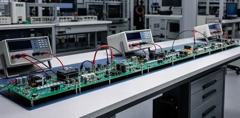
Choose copper, vias and layer geometry together
Increasing copper weight can reduce resistance, but it affects fabrication, etching, spacing, hole plating, stack-up, thermal balance and cost. The PCB copper-weight guide explains thickness options; the distribution design still needs a continuous geometry from source to load.
Treat neck-downs as part of the path
A wide plane that constricts at a fuse pad, connector, thermal relief, slot or via field may be governed by the narrow region. Inspect current-density transitions and how parallel paths share. Avoid assuming that current splits equally across vias or pins when geometry, contact, length or temperature differs.
Use the PCB via-current-capacity guide to frame via design inputs, then validate the actual array and fabrication assumptions. Place enough transitions, spread them to reduce local concentration where appropriate, and preserve return proximity.
Check temperature as well as resistance
Electrical drop and temperature reinforce each other because copper and contact resistance rise with temperature. Estimate board environment, airflow, nearby heat sources and enclosure constraints. Evaluate conductor heating, connector temperature and temperature-sensitive protection together.
Heavy copper may be justified for sustained high current, but a busbar, cable feed, additional connector or local converter can be a better architecture when distance dominates. The heavy copper PCB design guide covers manufacturability implications. Compare solutions on voltage margin, heat, assembly, service and fault behavior—not copper area alone.
Keep copper balance and board-shape risk visible on a large outline. A massive one-sided power region can interact with lamination and assembly temperature. Coordinate the electrical solution with stack-up and mechanical support before release.
Place feed points, connectors and protection deliberately
Feed architecture sets path length. A single end feed is simple and easy to fuse, but the farthest load sees the largest shared path. A center feed can halve maximum distance for symmetric loads. Multiple distributed feeds can reduce drop further but introduce current sharing, connector sequencing, fault isolation and reverse-current questions.
Compare end, center and distributed feeds
Build three simplified resistance networks using the same load states. Calculate node voltages and current in each connector/path. Include the return architecture. A distributed positive feed with one distant shared return can leave the original problem intact.
If two supplies or connectors can energize one plane, define whether they are paralleled, diode/ideal-diode isolated, switched or never simultaneous. Analyze backfeed and ground-potential differences during mating, fault and service.
Make faults and service states predictable
Place fuses or protection so conductor and connector ratings are protected in every energization path. Confirm interrupt rating, inrush, trip tolerance and thermal environment. A branch protection device also adds resistance; include its maximum relevant drop in the budget.
Choose connector pins based on current, derating, contact resistance, mating cycles, temperature, plating and harness distribution. Do not assign many parallel pins and assume perfect sharing. Symmetric copper approach, crimp/wire geometry and contact condition affect the result.
Define service behavior: which connector is safe to disconnect, whether hot-plug occurs, how stored energy discharges and how technicians verify a de-energized board. Label test points and protect them from accidental shorts.
Architecture rule: Every additional feed point needs a documented current-sharing, protection, backfeed and service answer.
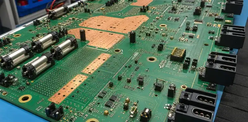
Preserve return paths and local energy
Power distribution is not purely DC. Switching loads draw high-frequency current through finite inductance, and a distant bulk supply cannot instantly support a local edge. Place local bulk and high-frequency decoupling according to the device or converter requirements, with compact loops between supply and return.
TI’s Practical PCB Design Rules emphasizes functional placement, ground-reference continuity and the problems created when returns detour around plane gaps. Analog Devices similarly discusses return-current behavior and grounding vias in mixed-signal layouts. For a large board, the physical distance makes deliberate local grouping even more valuable.
Keep high di/dt loops compact around converters, switches and loads. Do not route their outgoing current beside an unrelated or interrupted return. Preserve reference planes beneath sensitive signals and avoid forcing their return across high-current voltage gradients.
Separate DC distribution analysis from high-frequency impedance, then verify they coexist in the stack-up. A broad plane can offer low DC resistance but still be disrupted by slots, connector transitions or sparse stitching. Local capacitors reduce transient droop but cannot correct a continuous DC loss.
Define capacitor voltage, capacitance tolerance, ESR, ripple current, temperature and discharge behavior. Locate bulk energy near pulsed loads when useful, but ensure protection and inrush remain acceptable. A large capacitor at the far end may create a startup current that worsens the connector and plane drop it was intended to solve.
Review return-current paths with the signal and control teams. A sensor referencing local ground and reporting to a controller at source ground sees the difference between those nodes unless the interface is designed for it.
Keep sensing and low-level circuits out of power error
High current creates voltage differences on conductors labeled with the same ground net. Sensitive analog measurement, current sense, communication thresholds and regulator feedback can therefore report or regulate the wrong point if references share power drop.
Reference measurements intentionally
Define where every voltage specification is measured and where the instrument return connects. Use Kelvin connections for shunts or remote-sense points where the component/regulator documentation supports them. Route sense pairs away from noisy power loops and prevent load current from flowing through the sense conductor.
TI’s ground-bounce article illustrates how long thin returns, absent planes and distant sense components create error; it also describes Kelvin connection and local decoupling principles. Apply the topology, not the example’s device-specific dimensions.
Separate noisy loops without breaking returns
Partition placement so high-current switching, motors and relays do not share sensitive analog space. Separation does not mean arbitrary ground-plane cuts. A split that forces a signal return to detour can increase noise. Join domains according to the circuit’s reference and safety architecture, with controlled connection points when needed.
Protect ADC references, thermocouple circuits, current monitors and communication transceivers from local ground lift. Differential measurement can reject some common shift only inside its input common-mode and transient limits. Confirm those limits at worst load state.
On the schematic and test plan, use node names that reveal location—such as 24V_IN, 24V_MID, 24V_FAR, GND_SOURCE and GND_FAR_TEST—rather than one idealized rail label. The naming prompts reviewers to ask where margin is measured.
Measurement check: Reject any voltage-margin claim that omits the probe reference, operating state or physical node where the value applies.

Validate the board under real load combinations
Prototype validation should measure the source, intermediate branches and farthest loads simultaneously under defined states. Use suitable differential probes or isolated instruments where ground offsets make ordinary probing unsafe or misleading. Record supply setting, ambient, airflow, enclosure, firmware and harness.
Create a matrix that includes minimum/maximum supply tolerance, standby, startup, maximum continuous demand, pulsed demand, one-branch fault where safe, and recovery after a load step. Measure positive rail and local return so the round-trip behavior is visible. Capture transient minimum/maximum as well as steady averages.
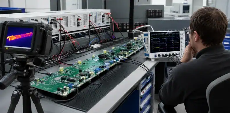
Use thermal imaging or contact sensors to locate connector pins, fuses, neck-downs, via fields and copper transitions that run hotter than the surrounding plane. Confirm emissivity/measurement limitations and follow with product-relevant sensors where needed. Compare measured loss with the calculated segment budget; large disagreement suggests an omitted contact or current-sharing issue.
Repeat after thermal equilibrium. A room-temperature pass can lose margin as connector and copper resistance rise. Challenge tolerances with production-representative assemblies rather than one hand-modified ideal sample.
Document acceptance per node and state, plus measurement location photographs. A single “24 V passed” line cannot prove that the far load remained above its minimum. Tie findings to drawing or stack-up changes and re-run affected cases.
Feed the validated limits into the large PCB first-article plan so production checks input polarity, connector build, rail voltages and thermal evidence without repeating full design validation on every lot.
| Validation record | Minimum context | Release question |
|---|---|---|
| Node-voltage capture | Supply, load state and reference point | Did every distant load retain margin? |
| Thermal result | Ambient, airflow and time to equilibrium | Did any connector or neck-down overheat? |
| Exception/change log | Board, connector and firmware revision | Does the measured baseline still apply? |
Record rule: Reopen the power budget whenever load sequencing, feed hardware, copper geometry or measurement references change.
Request a buildable power-distribution review
Send schematic, PCB/ODB++ data, stack-up, copper weight, finished dimensions, current-state table, node-voltage limits, connector/harness details, protection devices, environmental/airflow constraints and measurement/test expectations. Identify safety, isolation or regulatory requirements that affect routing and spacing.
Ask the manufacturer/assembler to review:
- copper thickness availability and tolerance in the selected large-board construction;
- minimum manufacturable neck-downs, clearances and plane registration;
- via arrays, finished holes and plating evidence for high-current transitions;
- connector, busbar or heavy-hardware assembly and support;
- copper-balance, board-shape and thermal-process implications;
- test access for source, branch and far-node measurements;
- first-article records and change triggers.
Keep electrical design responsibility explicit. A fabricator can review manufacturability and provide construction data, but the customer/system team owns load definition, acceptable drop, protection logic and functional safety unless the engineering scope says otherwise.
Request alternatives when the original geometry has weak margin: heavier copper, shorter route, more layers, distributed feed, busbar, cable, local conversion or connector changes. Compare cost and risk using the same node-voltage and temperature criteria.
Engineering review request: Submit the load-state table, schematic, stack-up, copper/via paths, connector data and required node measurements using the QueenEMS Large Format PCB page. A manufacturability response should identify current-path bottlenecks and name the first-article measurements that will verify them.
Define repeat-order validation triggers
Reopen the affected calculation and test cases when a connector, fuse, copper weight, stack-up, via array, feed location, harness, power supply, load, firmware sequence, enclosure or airflow changes. A substitution that preserves schematic net names can still change milliohms, temperature or current sharing.
Classify the change by path. Geometry or copper changes require resistance and thermal review; load or sequence changes require state-table review; sensing or reference changes require measurement and control-loop review. If several categories move together, repeat the integrated node-voltage and temperature matrix rather than approving isolated evidence.
Preserve the validated board revision, test setup, node photographs, raw captures and acceptance margins. The repeat-order team can then distinguish a controlled substitution from a new distribution architecture.
Change check: Repeat the integrated voltage and thermal validation when a change alters more than one feed, load, return or sensing assumption.
FAQ
Why does voltage fall at the far end of a long PCB?
Current flows through finite resistance in connectors, protection, copper, vias and the return path. The resulting I x R losses accumulate, and local ground can also shift relative to the source.
Is heavier copper always the best solution?
No. It may reduce plane resistance, but a connector, via field or neck-down can still dominate. Distributed feeds, busbars, local conversion or a shorter architecture may provide better overall margin.
Should a large board be fed from the center?
Center feed can reduce maximum path length for symmetric loads, but the right choice depends on load placement, protection, connector access, return paths and service behavior. Compare calculated networks.
Where should remote sense connect?
Follow the regulator documentation and sense the node the system must regulate, using a controlled low-current connection and matching reference. Analyze open-sense, noise and fault behavior.
What should be measured on the first prototype?
Measure source, branch and distant node voltages plus local returns, transient droop and temperatures at connectors, protection, neck-downs and via transitions under representative load combinations.
Sources
Written by the QueenEMS Engineering Team
Upload your files today · Free DFM check before production · Ship worldwide
Get your PCB prototypes in as fast as 24 hours. We handle FR4, Rogers, and hybrid boards up to 40 layers in volume production, with advanced builds subject to engineering review — free prototypes for 2–4 layer FR-4 boards, no minimum order.
Just upload your Gerber + BOM — we source every part, assemble, and inspect (AOI + X‑Ray) so you don't have to chase suppliers. Boards ship in as fast as 24 hours.