
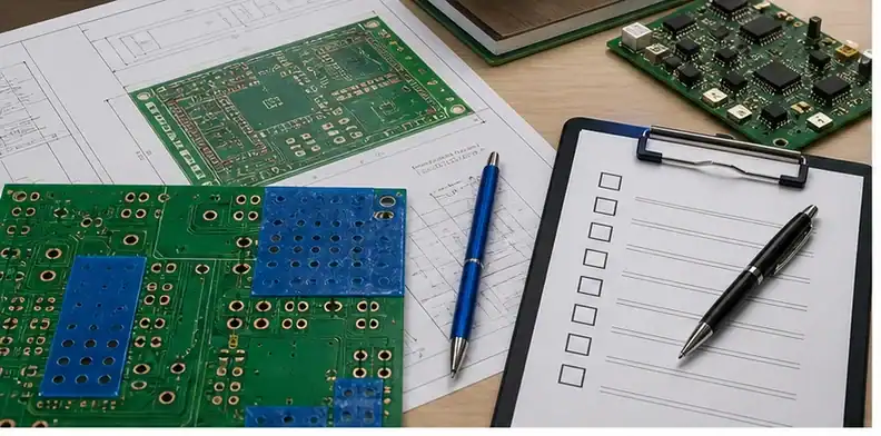
Quick answer: Peelable solder mask is a temporary process material, so the RFQ must define protected areas, process exposures, removal owner, and post-removal acceptance. A colored patch on a screenshot does not control edge overlap, curing, residue, or damage.
Key takeaways
• Tie each masked region to a named assembly operation.
• Send a dedicated layer with board outline and side identification.
• Approve the material data sheet and cure window for the chosen process.
• Separate application requirements from removal acceptance evidence.
Peelable-mask search results mix repair products, wave-solder protection, conformal-coating masking, and permanent solder resist. Before requesting price, identify the exact process step and the condition in which the board must leave the responsible supplier.
This page controls temporary-mask application and purchasing scope. It does not replace a material technical data sheet, and it deliberately separates application requirements from the downstream removal-acceptance page.
The buyer question behind this topic is usually practical: will the protected features still be usable after soldering or shipping? The article therefore keeps the focus on the process purpose, not the material name alone. A supplier can apply peelable mask, but the buyer must define what the mask protects and when it comes off.
Protection decision path
- When is peelable solder mask the right control?
- What areas should the drawing identify?
- How do thickness, curing, and removal affect quality?
- What assembly risks should buyers discuss?
- How should evidence be matched to risk?
- What belongs in the peelable-mask RFQ?
When is peelable solder mask the right control?
Peelable solder mask is useful when selected pads, holes, gold areas, or test points need temporary protection during soldering, wave solder, conformal coating, handling, or shipping. It should not be requested as a generic quality upgrade. The buyer should identify the process step it protects and the features that must be clean after removal.
SERP and AI answers often describe peelable mask as temporary resist or blue glue that protects pads or holes and is removed after soldering or another process step. The RFQ should therefore define three practical items: which features are protected, who removes the mask, and what counts as clean removal. Residue, tearing, or unclear removal responsibility can create the real assembly risk, even when the application itself is simple.
The quotation should name where temporary mask is applied, which process it must survive, and who removes it. Those three facts control labor and material choice; leaving any one unstated can move the task from PCB fabrication to assembly without either supplier pricing it.
When the same order includes assembly, connect the requirement to the PCBA RFQ files so the PCB and assembly assumptions do not split. If the peelable mask is only on the bare board drawing, the assembler may not know whether removal is expected before or after a process step.
What areas should the drawing identify?
The drawing should mark the protected areas clearly and state whether the mask covers pads, holes, connectors, gold fingers, tooling areas, or test points. It should also define keepout from fine-pitch features where residue or misregistration would be costly. A broad note such as peelable mask required can lead to over-coverage or missed critical pads.
CAM may tidy the application artwork, but it must not extend temporary mask across a test point, solderable termination, connector interface, or conformal-coating boundary without approval. The process owner should compare the proposed mask layer with the assembly sequence before release.
For final evidence, use PCB quality documents before shipment as the support page. If the mask is removed before shipment, request photos or inspection notes only for the features where residue would create real assembly risk.
How do thickness, curing, and removal affect quality?
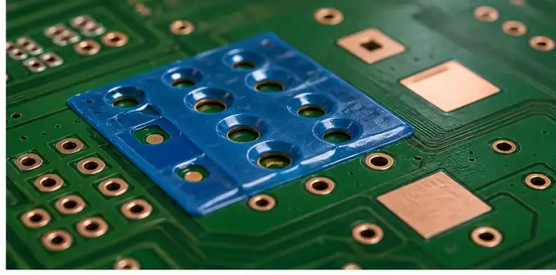
Peelable material must be thick enough to remove cleanly, cured enough to survive the protected process, and placed accurately enough to avoid covering solderable features that need exposure. If it is too thin, it may tear. If it is too broad, it may interfere with assembly. If it is poorly cured or stored, residue can become the real problem.
Thickness and cure cannot be borrowed from a generic internet table. For example, the MG Chemicals 862 technical data sheet specifies its own recommended application thickness and cure conditions; another formulation may require a different window. The approved product data sheet should control the job.
What assembly risks should buyers discuss?
The buyer should discuss whether the mask is removed before shipment, after receiving, or at the assembly site. That decision affects packaging, inspection, and responsibility. If the PCB supplier removes it, the buyer can request evidence that protected pads are clean. If the assembler removes it, instructions and handling become more important.
Evidence should follow the removal risk. A low-risk wave-solder shield may need application and after-peel photographs, while contacts, gold fingers, or coating edges can justify closer residue, surface-damage, and functional inspection after removal.
How should evidence be matched to risk?
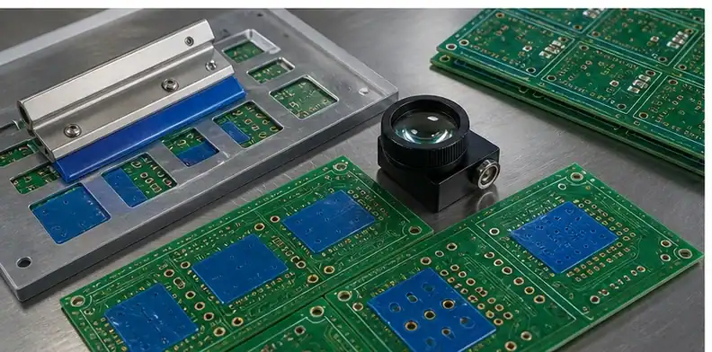
For low-risk prototype protection, a simple visual check may be enough. For production or customer-audited boards, sample photos, removal confirmation, or outgoing inspection records may be useful. Evidence should focus on clean removal and correct coverage, not on paperwork that does not answer the buyer’s process risk.
If masking labor is high, change the geometry or process deliberately. A reusable fixture, solder pallet, revised component sequence, or smaller protected zone may cost less than hand-applied mask, but each alternative changes what is exposed during soldering or coating and requires process approval.
What belongs in the peelable-mask RFQ?
Create a separate top or bottom temporary-mask layer and include the board outline on that layer. Give every protected area a clear boundary, reference dimensions or datum relationship, and a note stating whether the artwork depicts the mask edge or the protected keep-clear region.
List the reason for each region: exclude solder during wave, keep flux from a contact, protect gold fingers, shield a card edge, prevent coating on a connector interface, or support a rework step. Similar-looking shapes can need different materials and removal timing.
State the downstream exposures in order, including preheat, soldering, cleaning, conformal coating, storage, and any repeat thermal cycle. The supplier can only check material compatibility when it knows the temperature, chemistry, dwell, and sequence that the temporary mask will actually encounter.
Identify the approved material or ask the supplier to propose one with its technical data sheet. Review cure indication, application method, thickness window, compatibility with copper and finishes, storage limits, and removal instructions. Do not convert one vendor’s product values into a universal QueenEMS capability claim.
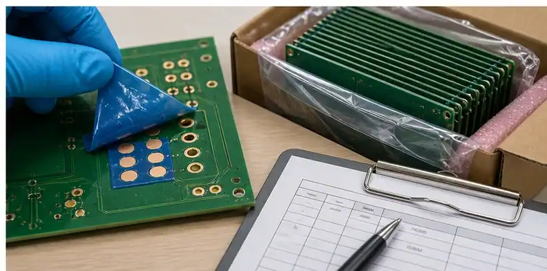
Define boundary acceptance where the mask overlaps permanent solder mask or a later coating. Removal can tear a coating edge if timing and overlap are poorly planned. The drawing should show which interface must remain clean and whether a controlled knife line or alternative masking method is permitted.
Assign removal ownership explicitly: PCB factory, assembly factory, conformal-coating supplier, or customer. State the process milestone for peeling and how removed boards are protected afterward. A requirement to “ship with blue mask” is fundamentally different from “remove after wave solder and inspect contacts.”
Keep the requirements page paired with the more specific peelable solder mask removal acceptance record. The first controls what is applied and why; the second controls residue, tearing, surface condition, and evidence after peeling. They support different buyer decisions and should not be merged.
Before production, approve a representative first-off image showing coverage and edge placement. After the relevant process, capture the condition that matters: complete removal, protected-pad cleanliness, undamaged finish, or coating-edge integrity. Avoid requesting unrelated certificates that do not demonstrate this local result.
Send the mask artwork with the assembly quote file set, material preference, process flow, quantity, and removal responsibility. This lets QueenEMS quote the labor at the correct manufacturing stage instead of treating it as an unpriced note.
Temporary mask terminology is a common source of scope error. Separate peelable latex or polymer masking from permanent LPI solder mask, removable tape, plugs, solder pallets, and peelable legend-like coatings. The quotation should identify the actual material class and the process in which it is used.
Artwork needs a manufacturing interpretation. State whether the drawn polygon is the deposited region, the minimum protected area, or a keepout boundary for the material. Add side and orientation references so a supplier cannot mirror the layer while preparing a panel.
Application around through-holes requires special thought. Material can bridge an opening, enter the barrel, or leave a thin tear-prone membrane. If the hole must remain solderable, testable, vented, or clean, show the permitted relationship between the mask edge and the finished opening.
Cure state affects both process resistance and removal. Ask how operators recognize complete cure and how they prevent an under-cured material from contaminating equipment or an overexposed patch from becoming difficult to peel. The approved data sheet and work instruction should answer these questions.
Thermal exposure should include cumulative history, not only peak temperature. A board may see preheat, wave solder, touch-up, bake, and coating cure before removal. The chosen material must remain protective and removable across the complete sequence used for this assembly.
Cleaning compatibility is equally project-specific. A cured mask may resist one flux remover or aqueous wash but respond differently to another chemistry. Name the cleaning process and ask the supplier to confirm it against the proposed material rather than assuming all peelable masks behave alike.
Edge design influences removal quality. Provide a reachable pull area where feasible and avoid thin isolated islands that can tear into fragments. When a protected zone is densely interrupted by pads or holes, discuss whether a fixture or tape gives more predictable removal than deposited mask.
Gold fingers and contact surfaces need acceptance after the material is gone. Define whether light discoloration, residue visible under magnification, adhesive traces, scratches, or coating lift are allowed. A simple before-and-after image can then be evaluated against a real criterion.
Packaging can become part of the requirement when mask remains on the shipped board. State storage duration, temperature limits, stacking protection, and latest removal date if the material ages in place. The receiving site needs the product identity and safe removal instruction.
When the PCB factory applies mask for a later assembler, both suppliers should approve the same sample. The fabricator controls deposition and cure; the assembler owns soldering exposure and removal. A split-scope process fails easily if either side reviews only its own step.
A first article should use the production panel, application equipment, cure profile, and downstream process whenever possible. Hand-applying a laboratory sample can prove basic compatibility but may not represent deposited thickness, edge repeatability, or operator removal on volume builds.
Close the order record with material lot or product identification when traceability matters, the approved artwork revision, application side, removal owner, and acceptance evidence. This compact set makes a repeat build safer than preserving dozens of informal photos without context.
Check whether temporary mask interferes with automated optical inspection, in-circuit test, flying probe, serialization, or barcode reading. If those operations occur before removal, the mask artwork must leave the required optical and electrical access even when solder protection is its primary purpose.
Operator safety and disposal follow the selected product’s documentation. Purchasing should obtain the current safety data sheet and confirm that the responsible factory can store, apply, cure, remove, and discard the material under its controlled process; the blog must not substitute for those instructions.
A good quotation response names the material, application method, cure control, protected process, removal milestone, and evidence. If the supplier answers only that blue mask is available, the buyer still lacks the information needed to compare scope or approve a production route.
Avoid treating color as a material specification. Blue, green, pink, or another appearance may help operators identify coverage, but chemistry and cured properties determine suitability. The purchase record should use a product identity or approved technical requirements, with color serving only as an inspection aid where applicable.
If the protected area contains a test pad needed later, define when access returns and how residue is checked before test. A mask can succeed during soldering yet create an electrical-contact problem at in-circuit test if removal and cleaning are not part of the same process plan.
Record permitted rework. Adding more material over a thin spot, trimming an edge, or reapplying after an early peel may be acceptable only before certain thermal or coating steps. The work instruction should prevent an operator from improvising a repair that changes cleanliness or removal behavior.
FAQ
Is PCB peelable solder mask requirements required for every PCB order?
No. It is relevant only when a temporary protective layer is part of fabrication, soldering, coating, repair, or shipping. Permanent solder mask openings belong in the ordinary solder-mask data and should not be mixed with this requirement.
Can the supplier decide the final detail during CAM?
The supplier may propose application margins and a compatible material, but the owner of the soldering or coating process must approve coverage, exposure, removal timing, and acceptance. CAM cannot see every downstream chemical or thermal step from Gerbers alone.
Who should remove peelable solder mask?
Choose the site immediately after the last process that needs protection and before the material or overlapping coating becomes difficult to peel cleanly. Put that owner and milestone in the purchase package so the board is not shipped in an unintended state.
What should QueenEMS review before quoting?
QueenEMS should review the mask layer, side, protected function, assembly sequence, proposed product data sheet, application method, removal site, and post-peel evidence. Contacts and cosmetic surfaces deserve an explicit acceptance statement.
To price temporary masking without assumptions, send QueenEMS the dedicated mask layer and process sequence. Highlight gold fingers, contacts, coating interfaces, and the party expected to peel and inspect the material.
Upload your files today · Free DFM check before production · Ship worldwide
Get your PCB prototypes in as fast as 24 hours. We handle FR4, Rogers, and Flex up to 60 layers — free prototypes for 2–4 layer boards, no minimum order.
Just upload your Gerber + BOM — we source every part, assemble, and inspect (AOI + X‑Ray) so you don't have to chase suppliers. Boards ship in as fast as 24 hours.