
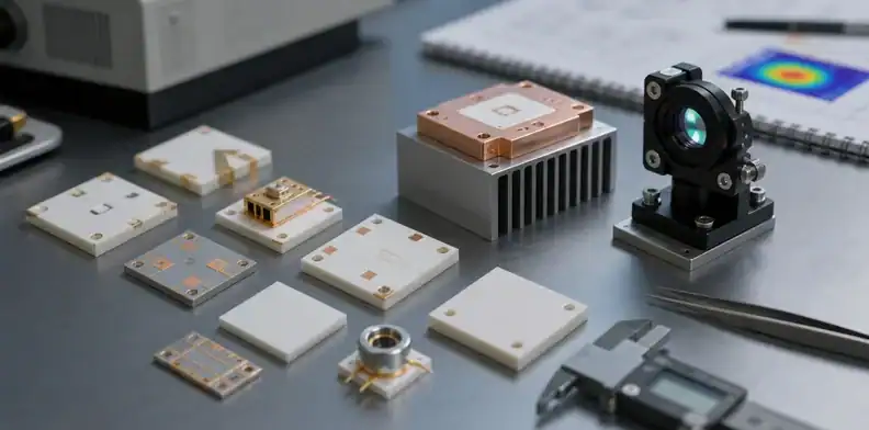
Quick Answer: A ceramic PCB for laser diodes should be selected by heat density, CTE match, flatness, die-attach or package interface, and optical alignment risk. Alumina can fit lower-power or cost-sensitive optical boards, while AlN, thin-film ceramic, or DPC-style ceramic routes may be needed when the laser source produces high local heat or the module has tight alignment and stability requirements. The RFQ should define laser package, wavelength, drive current, heat sink, substrate material, copper or metallization route, finish, flatness, assembly boundary, and inspection evidence before price is compared.
Laser diode projects often need flatness and metallization review early, so QueenEMS offers custom ceramic PCB service support before prototype release.
- Laser diode ceramic PCB decisions are driven by local heat and alignment stability, not by board outline alone.
- AlN is reviewed when thermal spreading becomes the bottleneck; thin-film or DPC routes may matter when geometry and pads are tight.
- The supplier should answer with material, metallization, finish, flatness, assembly, and inspection evidence, not only a ceramic quote.
Laser diode and optical module projects can look deceptively small. A board may only carry one emitter, a photodiode, a driver connection, or a compact optical subassembly. Yet the thermal and mechanical sensitivity can be higher than a much larger LED or power board because the heat source is concentrated and the optical path may tolerate little movement.
The LED and UV-C substrate discussion covers related thermal and optical-material questions. A laser module also needs the emitter position, attachment surface and optical reference to remain compatible as the assembly heats, cools and is mounted.
Table of Contents
- What does a ceramic PCB do for laser diode modules?
- When is alumina enough for an optical module?
- When should AlN or DPC ceramic enter the shortlist?
- How do CTE, flatness, and alignment change the RFQ?
- What metallization and finish details matter for laser diode assembly?
- What evidence should buyers request before prototype or production?
- When should the driver PCB stay separate from the laser submount?
- How should overseas buyers choose the right optical module partner?
What does a ceramic PCB do for laser diode modules?
A ceramic PCB for laser diode modules gives the emitter a stable electrical carrier, heat path, and mechanical interface. The board or substrate must move heat away from a small source area while preserving pad position, planarity, and attachment conditions that affect optical alignment.
The Hamamatsu L11854 pulsed-laser data sheet makes temperature sensitivity explicit with a wavelength-temperature coefficient for its identified parts and pulse conditions. That is a component example, not a universal value for all laser diodes. Use the selected emitter’s temperature-dependent characteristics and package thermal limits when choosing the substrate and cooling arrangement.
The buyer should begin with the laser package. A TO-can module, chip-on-submount assembly, optical transceiver subassembly, pump laser, sensing module, or laser diode array may need a different substrate route. The useful RFQ names the package, drive current, duty cycle, heat sink, optical alignment feature, and whether the supplier handles bare substrate only or also assembly.
Small geometry is another difference. A laser submount can have only a few pads yet require close control of their location, surface condition and suitability for wire bonding or die attachment. Experience producing a ceramic heater does not by itself establish the ability to hold the drawing’s optical reference dimensions after assembly.
When is alumina enough for an optical module?
Alumina can be enough when the laser diode power is moderate, the heat sink has margin, the layout is not extremely dense, and the assembly interface does not require a higher thermal ceramic. It is a mature, widely available ceramic material for many insulated submounts and optical support circuits.
Use the Ceramic PCB Guide to separate substrate and metallization choices, then check optical flatness and die-attach limits before a nominal W/mK value drives the laser-module decision.
Alumina may also be the practical route for prototypes that are still proving optical fit, driver behavior, or enclosure design. When the project is early, a fast and well-documented alumina sample may teach the team more than an expensive material upgrade made before the thermal bottleneck is understood.
The buyer should still define the limits. Ask for ceramic thickness, copper or metallization route, finished thickness, surface finish, flatness or bow/twist expectation, outline method, and assembly exposure. A quote that simply says “alumina ceramic PCB” leaves too much room for hidden differences between suppliers.
| Alumina fit signal | Buyer check |
|---|---|
| Moderate laser heat | Package temperature has margin in the intended heat sink |
| Simple optical support board | Alignment is not controlled mainly by the substrate surface |
| Early prototype | The design is still proving mechanics or firmware |
| Cost-sensitive module | Thermal and stability data support the lower-cost ceramic |
Alumina should not be rejected because AlN sounds more advanced. It should be rejected only when the measured or modeled thermal path, flatness, or alignment condition shows that alumina does not leave enough margin.
When should AlN or DPC ceramic enter the shortlist?
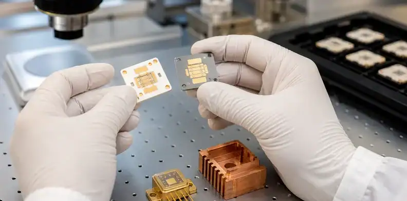
AlN is a ceramic material; DPC and thin film describe metallization routes. They are separate choices and may be combined. Kyocera’s thin-film laser submount page describes AlN and also offers alumina, with examples including side metallization and deposited AuSn. This supports comparing a particular material/metal stack against the package requirement, not declaring one process necessary for every laser.
Typical triggers include laser diode arrays, pump laser modules, high-duty operation, compact transceiver assemblies, or a design where the laser source sits close to temperature-sensitive optics or detectors. In those cases, a few degrees of thermal margin can affect wavelength stability, output behavior, or calibration drift.
The buyer should not ask suppliers to “quote AlN” without explaining the problem AlN must solve. A better RFQ says that the thermal model or early sample shows local hot-spot risk, then asks the supplier to quote AlN with material grade or thermal class, thickness, metallization route, finish, flatness, and assembly notes.
DPC or thin-film ceramic may be relevant when the limiting issue is not only bulk thermal conductivity but pad precision, plated vias, fine lines, surface finish, or compatibility with a package interface. The manufacturing route should follow the feature set. A thick copper power-substrate answer may be wrong for a fine optical submount.
How do CTE, flatness, and alignment change the RFQ?
CTE, flatness, and alignment change the laser diode RFQ because the board may become part of the optical reference structure. A substrate that is electrically correct can still cause trouble if it bends, shifts, or stresses the package during soldering, mounting, or thermal cycling.
CTE mismatch matters when ceramic, copper, solder, package base, heat sink, and enclosure materials expand at different rates. The risk is not only cracking. It can also be solder fatigue, die attach stress, loss of thermal contact, or optical misalignment after repeated temperature changes.
Flatness belongs in the drawing. Laser diode submounts and optical modules may need controlled contact to a heat sink, carrier, or optical bench. If the drawing does not state flatness or mounting assumptions, the supplier may quote a board that passes its own ceramic process but fails the module assembly.
Alignment notes should identify which features are functional. Mounting holes, slots, fiducials, substrate edges, copper pads, die attach locations, lens seats, or connector interfaces may require tighter control than ordinary PCB features. The buyer should mark those features in the drawing instead of leaving the supplier to guess.
Close the tolerance chain from cooler to optical axis
Start at a stable mounting datum and follow the stack through the cooler interface, substrate back face, ceramic and metal thickness, die-attach layer, die surface and emitting feature. Then connect the emitting feature to the lens or fiber reference. Specify which surface or feature controls height, tilt and lateral position. Overall board flatness alone does not close that chain.
For a concrete datum example, the L11854 data sheet defines optical-axis tilt from the bottom of the package base and emitter-position accuracy from the package-base centre. Those are component-specific references, not generic ceramic tolerances. Carry the chosen emitter’s own references into the carrier drawing before allocating the substrate and attachment tolerances.
| Assembly state | Feature to evaluate | What the result can establish |
|---|---|---|
| Bare finished substrate | Local die-pad plane and position relative to defined datums | The fabricated attachment interface |
| After die attachment | Die position, tilt and bondline relative to the same references | Placement plus the attachment contribution |
| After final mounting | Emitter-to-optic relationship at the specified mechanical and thermal condition | Whether the assembled optical reference remains within its requirement |
An illustrative height relation is z_emitter = z_mount + t_interface + t_substrate + t_metallization + t_attach + z_die-to-emitter, provided each term uses the same axis and physical definition. Do not add a copper layer twice if the supplier’s finished-substrate thickness already includes it. Use signed tolerances from the actual drawings; a worst-case sum and a statistical estimate answer different questions and require different assumptions.
Recheck the chain after changing attachment material or substrate thickness. A thinner ceramic can improve one thermal term while moving the emitter relative to a fixed lens. Ask the photonics assembly owner whether passive dimensional control is sufficient or active alignment is required. A supplier’s bare-submount inspection cannot demonstrate the final optical coupling result.
For mechanical stress background, the QueenEMS article on ceramic PCB CTE and cracking during assembly is useful. For laser modules, the key is not only crack prevention; it is maintaining the heat and optical reference path.
What metallization and finish details matter for laser diode assembly?
Metallization and finish matter because laser diode assemblies may use solder attach, eutectic attach, conductive epoxy, wire bonding, or connectorized package mounting. Each attachment route can require a different pad finish, surface quality, and thermal exposure.
For soldered packages, the buyer should identify solder alloy, reflow profile, stencil or preform assumptions, pad size, and inspection method. For die attach or submount work, the quote may need finish details, thickness expectations, wire-bond compatibility, cleanliness, and void-control assumptions. If a heat sink or carrier is part of the assembly, the interface should be shown in the drawing.
The supplier should state the copper or metallization process: DPC, thick film, thin film, plated copper, or another route. Those routes affect line width, adhesion, feature tolerance, finish options, and cost. A fine-pitch optical module may need a different route than a simple ceramic breakout board.
| Assembly route | RFQ detail to define |
|---|---|
| Soldered laser package | Finish, pad size, paste or preform, reflow profile |
| Eutectic or die attach | Finish stack, flatness, void expectation, cleaning |
| Wire bonding | Bondable finish and pad geometry |
| Heat-sink mounting | Backside flatness, contact area, mounting pressure |
| Optical alignment | Functional datums, fiducials, edge tolerance |
Use the prototype-file preparation guide for the fabrication package, then add the laser package drawing and optical-interface requirements.
What evidence should buyers request before prototype or production?
Buyers should request evidence that matches the optical-module risk: material statement, metallization route, finish stack, flatness or dimensional inspection, solderability or attach notes, packaging controls, and any test or inspection data tied to functional features.
For a prototype, the evidence may be limited but should still be explicit. A good supplier response states what is controlled, what is only estimated, and what needs engineering approval after sample testing. It should not hide uncertainty behind a generic “ceramic PCB prototype” line item.
For production, the evidence should become a release package. The drawing revision, material route, finish, flatness, functional datums, packaging, change-control rule, and assembly boundary should be locked. If the buyer tested an AlN sample but purchasing later orders an alumina quote, the production comparison is invalid.
| Evidence | Prototype need | Production need |
|---|---|---|
| Material and route | Named option | Locked to revision |
| Finish and attach notes | Supplier recommendation | Approved process record |
| Flatness and dimensions | Sample inspection | Controlled acceptance rule |
| Thermal assumption | Engineering estimate | Test or qualification record |
| Packaging | Basic protection | Lot labels and handling notes |
The supplier’s English DFM response is part of the evidence for overseas buyers. A clear answer should identify missing package data, questionable pad geometry, finish risk, heat-sink ambiguity, and any ceramic manufacturing limit before the order is released.
When should the driver PCB stay separate from the laser submount?
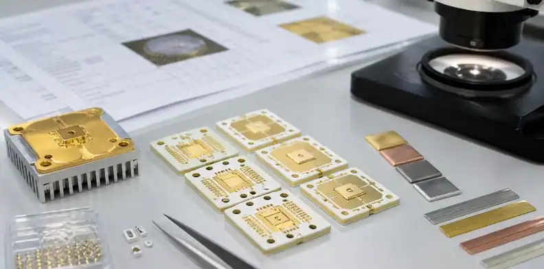
The driver PCB should stay separate when the laser submount needs a specialized ceramic route but the control electronics, connectors, protection circuits, or digital interface are better served by ordinary PCB materials. Many optical modules are not one board decision. They are a package or submount decision plus a driver, interconnect, and enclosure decision.
This separation can reduce cost and risk. The laser source may need AlN, DPC, thin-film ceramic, or a precision ceramic carrier, while the driver board may fit FR-4, high-Tg FR-4, or a controlled-impedance laminate. Forcing the whole assembly onto ceramic may make the quote expensive and harder to source without improving the part of the design that actually needs ceramic.
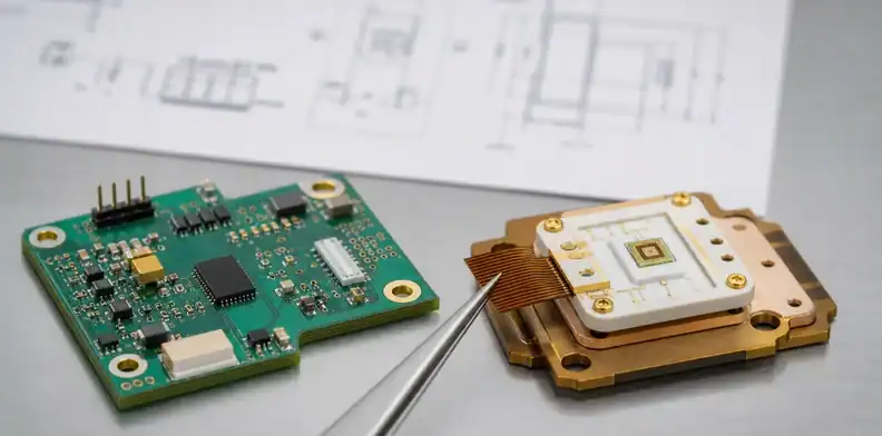
The RFQ should state where the ceramic deliverable ends. For example, the ceramic submount may include only the laser pads, thermal interface, and functional datums, while a separate PCB carries the driver IC, connector, protection components, and test pads. The interface between them then becomes the controlled item: wire bond, flex, soldered interposer, board-to-board connector, or cable.
For a broader material boundary, use the QueenEMS article on ceramic PCB vs FR-4 cost premium. For laser modules, the cost question should be tied to the optical and thermal subassembly rather than the entire control board.
Use one substrate only when the electrical, thermal, and mechanical benefits justify the complexity. Use a split design when the ceramic part protects the laser path and the PCB part handles the ordinary electronics more efficiently.
How should overseas buyers choose the right optical module partner?
Overseas buyers should choose the partner by deliverable: bare ceramic substrate, patterned ceramic PCB, laser submount, assembled optical module, or PCB/PCBA handoff. Those deliverables need different suppliers and different evidence.
A specialist ceramic substrate supplier may be ideal for high-volume material or submount production. A photonics package house may be needed for die attach, wire bonding, sealing, or optical alignment. An export-facing PCB/PCBA partner becomes useful when the buyer needs a small build, fabrication plus assembly coordination, English DFM, and documentation support.
QueenEMS fits the last category best. The role is to help overseas buyers turn laser diode or optical module files into a controlled RFQ: review whether alumina, AlN, DPC, thin-film ceramic, or another route is quote-ready; check missing package and thermal inputs; coordinate PCB fabrication and PCBA when appropriate; and keep supplier assumptions visible.
The best first email includes the laser package datasheet, wavelength, power or drive condition, Gerber or ODB++ files, fabrication drawing, heat sink interface, optical alignment notes, target substrate material if known, finish preference, assembly scope, quantity, and evidence requirements. That package lets the supplier answer technically instead of guessing from a board outline.
FAQ
Is AlN always better for laser diode ceramic PCB?
No. AlN is useful when thermal spreading is the bottleneck, but alumina can fit lower-power or cost-sensitive optical boards. The decision should follow heat density, package interface, flatness, and alignment risk.
What is the best ceramic PCB material for laser diode modules?
There is no universal best ceramic material. Compare identified alumina and AlN grades against heat flow and mechanical requirements, then specify the metallization process, attachment surface and package geometry separately. DPC and thin film are process choices, not additional ceramic materials.
What should I send for a laser diode ceramic PCB quote?
Send Gerber or ODB++ files, fabrication drawing, laser package datasheet, wavelength, drive current or power condition, heat sink drawing, flatness or datum notes, finish requirement, assembly scope, quantity, and evidence needs.
Can a normal ceramic PCB supplier build laser diode submounts?
Sometimes, but only if the supplier can meet the material, metallization, finish, flatness, and inspection requirements. Fine die-attach, wire bonding, or optical alignment work may require a more specialized route.
Why do laser diode boards crack or lose alignment?
Common causes include CTE mismatch, poor mounting support, unsuitable reflow or attach process, weak flatness control, heavy mechanical stress, or functional datums that were never defined in the drawing.
Send QueenEMS a laser diode ceramic PCB RFQ
Send the laser package drawing, drive conditions, substrate layout, heat-sink interface, optical datums, attachment process and inspection requirements through the QueenEMS optical-project inquiry page. Ask QueenEMS to quote the ceramic construction and define the handoff to any photonics assembly specialist. Final optical alignment and coupling verification should have an identified owner.
Sources
- Hamamatsu Photonics, Hamamatsu L11854 pulsed-laser data sheet
- Kyocera, Kyocera thin-film laser-diode submounts
Written by the QueenEMS Engineering Team
Upload your files today · Free DFM check before production · Ship worldwide
Get your PCB prototypes in as fast as 24 hours. We handle FR4, Rogers, and Flex up to 60 layers — free prototypes for 2–4 layer boards, no minimum order.
Just upload your Gerber + BOM — we source every part, assemble, and inspect (AOI + X‑Ray) so you don't have to chase suppliers. Boards ship in as fast as 24 hours.