
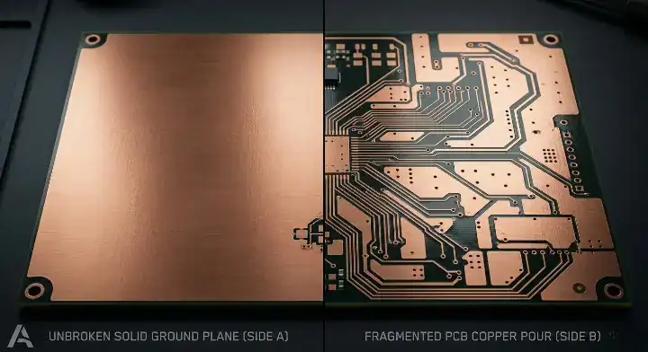
Quick Answer: PCB copper pour vs ground plane decisions should start with return-path continuity, not with how much empty copper looks available in CAD. A solid ground plane gives critical signals a continuous reference, while copper pour is a local fill that can help with copper balance, thermal spreading, shielding, or power distribution only when it is connected, stitched, and kept away from sensitive zones.
Key takeaways
- Copper pour is not automatically a ground plane.
- Floating or poorly stitched pour can become an EMI and crosstalk risk.
- Two-layer boards can use grounded pour, but dense/high-speed layouts often need a real reference layer.
- Before fabrication, review dead copper, split returns, antenna keep-outs, thermal relief, and impedance clearances.
PCB copper pour vs ground plane is one of those layout choices that looks simple until a board fails EMC testing, impedance control, or first-article inspection. Filling unused space with copper can be helpful, but it can also hide broken return paths and isolated islands that make the board noisier.
The practical rule is this: a copper pour is useful when it serves a defined electrical, thermal, or manufacturing purpose. A solid ground plane is useful when a signal needs a continuous low-impedance reference. Treating them as the same thing is where the trouble starts.
Table of Contents
- What Is PCB Copper Pour vs Ground Plane?
- How Do Return Paths Change the Decision?
- When Does a Two-Layer PCB Need Copper Pour?
- How Should Stitching Vias Control Copper Pour?
- Should Analog and Digital Grounds Be Split?
- How Does Copper Pour Affect Fabrication?
- When Should Copper Be Cleared Away?
- How Does Pour Affect Impedance and RF Layout?
- What Should Buyers Check Before Gerber Release?
- When Should QueenEMS Review the Stackup?
What Is PCB Copper Pour vs Ground Plane?
PCB copper pour is copper filled into unused areas of a routed layer. A ground plane is a continuous copper reference, usually on a dedicated layer, tied to the circuit ground. They can both be connected to the GND net, but they do not behave the same way.
The difference is physical continuity. A dedicated ground plane can sit under a signal layer with few interruptions. A copper pour on a routing layer must flow around pads, traces, vias, keep-outs, and component clearances. That makes it naturally fragmented.
| Feature | Copper pour | Solid ground plane |
|---|---|---|
| Location | Usually on signal or outer layers | Usually a dedicated internal layer |
| Continuity | Broken by routing and clearances | Intended to be broad and continuous |
| Main value | Copper balance, shielding, local current or heat spreading | Stable reference and return path |
| Main risk | Floating islands, random capacitance, poor stitching | Splits, slots, bad layer transitions |
| Best use | Local support after routing rules are checked | Primary reference for critical signals |
The search confusion is understandable. Many CAD tools let you pour a polygon and assign it to GND, so the screen looks like a plane. The manufacturing file, however, still contains a shaped copper region that may be chopped into islands. A real review asks whether the return current can move where the circuit needs it to move.
For a buyer, this matters because a PCB that “has ground copper everywhere” can still have poor EMC behavior. It also affects DFM review, because the fabricator must evaluate clearances, copper balance, drill spacing, solderability, and whether the final copper pattern matches the release intent.
How Do Return Paths Change the Decision?
Return paths change the decision because fast signals do not only need a route out; they also need a controlled route back. A solid reference plane usually gives the return current a short, predictable path, while a fragmented pour may force current around gaps and enlarge the loop area.
At low frequencies and slow edge rates, current distribution is often dominated by resistance. As frequency content rises, inductance and capacitance matter more. Altium’s return-path guidance emphasizes that a signal’s return path and the resulting loop inductance directly affect EMI susceptibility. In plain terms: the larger and less predictable the loop, the easier it is for the board to radiate or pick up noise.
This is why “more copper” is not automatically better. A copper shape placed near a trace can act as a local reference only if it is actually tied into the return system. If a signal crosses a slot, a split, or an isolated patch, the current may detour to find the nearest usable reference. That detour is often the real EMC problem.
Use this decision order:
- Identify clocks, fast digital edges, switch nodes, RF lines, ADC inputs, and cable-connected nets.
- Confirm each critical net has a continuous reference under or near the route.
- Check layer transitions for nearby return vias or decoupling paths.
- Add copper pour only where it improves a known return, shielding, thermal, or balance need.
- Remove copper where it creates islands, impedance surprises, or antenna keep-out violations.

When Does a Two-Layer PCB Need Copper Pour?
A two-layer PCB often needs copper pour because it does not have a dedicated internal reference layer. Grounded pour can improve local ground access, reduce long ground traces, balance copper, and help simple low-speed boards behave better.
The important word is “grounded.” Electrical Engineering Stack Exchange discussions show a common beginner misconception: copper pour does not automatically connect itself to ground unless the layout tool assigns it to the net and the geometry provides actual connections. A floating pour buys little and can create problems.
Two-layer copper pour is reasonable when:
- the board is low-speed or mostly DC/power control;
- component density leaves broad, connected copper regions;
- ground pins can connect into the pour without thin bottlenecks;
- top and bottom pours are tied together with useful stitching vias;
- antenna, isolation, creepage, and analog keep-outs are respected.
It is less convincing when the board has dense routing, high-speed interfaces, strict EMC requirements, fine-pitch parts, or controlled-impedance traces. In those cases, a two-layer copper pour may look like a reference but behave like a patchwork of disconnected return options.
If the routing density already forces signals to cross many breaks, compare the cost of a four-layer stackup early. QueenEMS’ 2-layer vs 4-layer PCB guide is a useful companion when the sourcing question becomes cost versus EMC/debug risk.
How Should Stitching Vias Control Copper Pour?
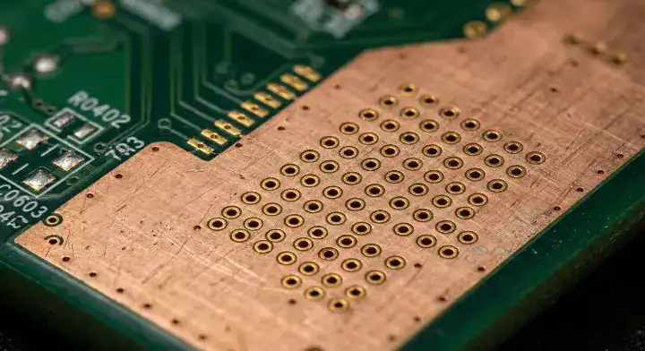
Stitching vias should connect copper pour to the intended reference system at useful intervals, near boundaries, and near layer transitions. They should not be scattered only for appearance; they must reduce return-path gaps, connect copper islands, and prevent loose copper from acting as an unwanted radiator.
Altium’s copper-pour guidance is blunt on one rule: if you use copper pour, ground it rather than leaving it floating. AllAboutCircuits adds the EMC nuance: leftover copper regions and dead copper can behave like antennas, and some isolated regions may be missed by automated tools.
Use stitching vias in five places:
- around board edges when the edge copper is part of a shield;
- near connectors and cable-entry areas where common-mode noise matters;
- beside signal layer transitions where the return path also changes layer;
- inside otherwise isolated copper patches that should remain connected;
- around RF or noisy zones, while still respecting antenna keep-outs.
Do not treat a universal via spacing number as law. A conservative EMC design may need tighter stitching than a slow industrial control board. A high-speed RF board may need simulation, field-solver support, or lab validation. The safer published guidance is to define the function of the stitching fence, then verify whether the geometry supports the board’s highest-risk signals.
For fabrication, stitching density also creates cost and manufacturability questions. Very dense via fields can affect drill count, annular ring margins, and yield. The right DFM check balances electrical intent with the fabricator’s via capabilities.
Should Analog and Digital Grounds Be Split?
Analog and digital grounds should usually be partitioned by placement and routing discipline, not by cutting a hard slot through the reference plane. A split can help in specific isolation cases, but a careless split often severs high-frequency return paths.
The old advice was simple: keep analog noise away from digital noise by splitting AGND and DGND. The more reliable modern question is different: where will each return current actually flow? If a fast digital trace crosses the split, the return current cannot travel under the trace. It detours around the gap, increasing loop area and radiated noise.
A better mixed-signal strategy is:
- place analog and digital components in distinct zones;
- keep noisy switch nodes and clocks away from sensitive inputs;
- route signals so they do not cross reference-plane gaps;
- connect converter grounds according to the IC vendor’s layout guidance;
- use a continuous reference where high-frequency return paths must stay short.
There are real exceptions. Galvanic isolation, high-voltage safety spacing, medical isolation, and certain power architectures may require physical separation. In those cases, the split is not a casual “noise trick”; it is a controlled safety or functional boundary with creepage, clearance, and test requirements.
When the design is mixed-signal and high-density, the stackup should be locked before routing. A late copper pour cannot rescue a layout where critical traces cross slots or where the reference layer is too far away from the signal layer.
How Does Copper Pour Affect Fabrication?
Copper pour affects fabrication through copper balance, plating distribution, solderability, thermal relief, and inspection clarity. It usually does not make a board faster to fabricate simply because more empty space was filled; the copper pattern is still manufactured through the same imaging, etching, and plating sequence.
Copper balance is a real manufacturing reason to pour. AllAboutCircuits notes that copper fill can help balance copper distribution across layers, which affects heat distribution during board fabrication. KiCad community discussions also point to dimensional stability and thermal management as practical reasons to use pours in some designs.
However, fabrication benefits are not automatic. Poorly designed pour can create:
- narrow acid traps or slivers that complicate etching;
- uneven copper distribution that affects flatness;
- too little clearance around pads and traces;
- soldering difficulty when pads connect solidly to large copper regions;
- unclear intent when isolated copper remains in Gerbers.
Thermal relief is a buyer-facing detail because it affects assembly. A pad tied directly to a large pour can be harder to heat during soldering or rework. A power pad or thermal pad may need a solid connection for current or heat, while small hand-soldered pins may need thermal spokes. The right answer depends on current, heat, assembly method, and inspection criteria.
If warpage is already a concern, connect copper decisions to the broader mechanical design. QueenEMS’ PCB warping causes guide explains why copper symmetry, thickness, panel design, and heat exposure should be reviewed together.
When Should Copper Be Cleared Away?
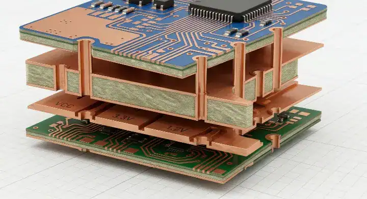
Copper should be cleared away when it violates a keep-out, changes impedance, traps noise, complicates soldering, or creates an isolated island with no useful connection. Removing copper is often a stronger engineering choice than filling every empty area.
Clear copper from RF antenna zones unless the antenna design specifically requires it. A small copper patch near a chip antenna or printed antenna can detune the match and alter the radiation pattern. Follow the RF module or antenna vendor’s keep-out drawings before using any automatic pour command.
Also consider clearing copper near:
- high-impedance analog sensor inputs;
- crystal oscillator guard areas where the IC vendor gives layout rules;
- controlled-impedance traces that were solved without nearby side copper;
- isolation barriers that require creepage and clearance;
- connector shield areas unless chassis bonding is intentional;
- areas where pour creates thin, fragile copper slivers.
AllAboutCircuits describes grounded copper pour as a double-edged sword because nearby copper can introduce unintended capacitance and alter impedance-controlled traces. That is the key tradeoff: copper can shield one problem while creating another.
The release rule is simple: every copper region needs a reason. If the reason is “CAD made it there,” delete it or connect it properly.
How Does Pour Affect Impedance and RF Layout?
Copper pour can affect impedance and RF layout by adding side capacitance, changing field distribution, and disturbing antenna or transmission-line assumptions. This is especially important when the trace width was calculated for a specific stackup and reference plane.
For controlled-impedance traces, the solver usually assumes a defined dielectric thickness, copper thickness, trace width, spacing, and reference plane. Nearby copper pour on the same layer can create coplanar coupling. That may be useful if it is part of the intended geometry, but it is a problem when the pour appears after the impedance calculation.
Practical checks:
- keep pour clearance wider around impedance-controlled traces unless the geometry is solved as coplanar;
- avoid chopped reference copper under high-speed routes;
- do not cross split planes with clock, RF, USB, Ethernet, LVDS, PCIe, or sensitive ADC/DAC routes;
- add return vias near signal vias when the reference layer changes;
- confirm RF keep-out zones before final polygon repour.
For high-speed products, pair this copper review with a stackup and impedance review. QueenEMS’ controlled impedance PCB guide explains how stackup geometry, copper thickness, dielectric height, and test coupons should be specified before production.

What Should Buyers Check Before Gerber Release?
Before Gerber release, buyers should check whether copper pour supports the design intent and whether the fabrication package makes that intent inspectable. Do not approve a layout just because the screen looks “filled.”
Use this release checklist:
| Check | What to verify | Why it matters |
|---|---|---|
| Net assignment | Pour is tied to GND, power, chassis, or another intended net | Prevents floating copper |
| Dead copper | Unconnected islands are removed or intentionally stitched | Reduces EMI and crosstalk risk |
| Reference continuity | Critical traces do not cross slots or split regions | Protects return paths |
| Stitching vias | Vias are placed near edges, transitions, and isolated regions | Connects pour to the ground system |
| Copper balance | Large layer imbalances are reviewed | Supports flatness and fabrication control |
| Thermal relief | Pads use thermal or solid connections as appropriate | Protects solderability and current/heat paths |
| Keep-outs | Antenna, isolation, and mechanical zones are respected | Prevents RF, safety, and fit failures |
| Impedance | Pour clearance matches solved geometry | Prevents unintended trace impedance shifts |
Also regenerate the pour after the last routing change. A layout may pass early review and then create islands after one late connector move. For production, the final exported Gerbers, drill files, stackup, and fabrication notes should all match the same revision.
If trace width, clearance, and copper pour rules are being adjusted together, use the PCB trace width and spacing guide as a companion checklist before sending files.
When Should QueenEMS Review the Stackup?
QueenEMS should review the stackup before fabrication when copper pour, ground plane continuity, impedance, EMC risk, or assembly heat flow can change the board outcome. The best time is before routing is frozen, not after the Gerbers are already released.
Send the review package when the design includes:
- two-layer boards with clocks, fast edges, connectors, or wireless modules;
- four-layer or higher boards with split planes or layer transitions;
- controlled-impedance nets or RF keep-outs;
- dense copper areas tied to thermal or power pads;
- high-current power regions and mixed-signal partitioning;
- EMC certification, medical, industrial, automotive, or cable-connected requirements.
QueenEMS can then review the board as a manufacturable package: stackup, copper balance, pour clearances, dead copper, via strategy, thermal relief, impedance intent, and assembly constraints. For designs moving beyond simple two-layer layouts, this review can also connect the layout decision to multilayer PCB manufacturing limits before the quote is finalized. This does not replace formal EMC testing or SI simulation, but it catches common release errors before they become a fabricated-board problem.
If your design is close to the 2-layer versus 4-layer boundary, send the stackup target, Gerbers, impedance requirements, fastest interfaces, RF module drawings, and assembly method through the QueenEMS contact page. QueenEMS can help compare whether copper pour rules are enough or whether a dedicated reference layer is the cleaner production choice.

FAQ
Is copper pour the same as a ground plane?
No. Copper pour is a filled copper region on a layer, while a ground plane is a broad continuous reference tied to ground. A pour can support ground only when it is connected and not badly fragmented.
Should copper pour be on the top or bottom layer?
Use the layer that gives the most useful continuous copper without violating routing, keep-out, or soldering rules. On two-layer boards, both layers may use grounded pour if they are stitched and audited.
Does copper pour reduce PCB manufacturing cost?
Usually not in a meaningful buyer-facing way. It may reduce etched copper removal, but board cost is more strongly driven by layers, material, drill count, finish, tolerances, panelization, and testing.
Can copper pour replace decoupling capacitors?
No. Copper pour can add some plane or local capacitance in certain stackups, but IC power pins still need properly placed decoupling capacitors and low-inductance return paths.
Should RF antenna areas have copper pour?
No, not unless the antenna or module documentation explicitly requires it. Most RF antenna designs need defined copper keep-outs, ground references, and matching geometry.
Sources
- Altium, The Copper Ground Pours Problem in PCB Designs
- Altium, Copper Pour and Via Stitching
- Altium, Follow Your Multilayer Ground Return Path to Prevent EMI
- AllAboutCircuits, The Good and Bad of Grounded Copper Pour
- Electrical Engineering Stack Exchange, A confusion on using PCB copper pour
- KiCad Forum, Newbie question: Benefit of copper pours?
Written by the QueenEMS Engineering Team
Upload your files today · Free DFM check before production · Ship worldwide
Get your PCB prototypes in as fast as 24 hours. We handle FR4, Rogers, and hybrid boards up to 40 layers in volume production, with advanced builds subject to engineering review — free prototypes for 2–4 layer FR-4 boards, no minimum order.
Just upload your Gerber + BOM — we source every part, assemble, and inspect (AOI + X‑Ray) so you don't have to chase suppliers. Boards ship in as fast as 24 hours.