
Quick Answer: PCB gold fingers are edge connectors plated with a hard gold alloy over a nickel barrier, providing highly durable contact surfaces for motherboards and expansion cards. Hard gold plating featuring 30µin to 50µin thickness withstands over 1,000 insertion cycles, whereas standard ENIG fails after just 10. You must maintain a minimum board thickness of 1.2mm to safely bevel the connector edges at standard 30-degree or 45-degree angles. Key takeaways:
- Hard gold plating contains 5% to 10% cobalt to increase mechanical wear resistance significantly.
- IPC-4556 standards mandate a minimum of 32µin thickness for high-reliability edge contacts.
- Inner layer copper must be pulled back to prevent exposure and shorting during the edge beveling process.
- Performing the ASTM B571 tape test on every batch verifies that the nickel-gold adhesion meets required durability thresholds.
A circuit board edge connector requires highly conductive, wear-resistant contacts to function inside a motherboard slot. When your field units fail due to worn-out connection points, you face massive product recall expenses and damaged client trust. Specifying high-quality PCB gold fingers actively prevents signal degradation across repetitive mating cycles, saving your hardware investment. This guide breaks down the design rules, exact plating specifications, and manufacturing processes required to build flawless edge connectors.
Table of Contents
- 1. What Are PCB Gold Fingers and Why Do Edge Connectors Need Them?
- 2. How Does the Plating Process for PCB Gold Fingers Work?
- 3. What Are the Design Rules for PCB Gold Fingers?
- 4. Hard Gold vs ENIG: Which Plating Should You Choose for PCB Gold Fingers?
- 5. How Do IPC-4556 Standards Control PCB Gold Fingers Quality?
- 6. What Are the Exact Costs Associated with PCB Gold Fingers?
- 7. What Are Common PCB Gold Fingers Manufacturing Defects and How to Prevent Them?
- 8. Why Is Inner Layer Copper Removal Required for PCB Gold Fingers?
- 9. How Do You Panelize Boards with PCB Gold Fingers for Assembly?
- 10. When Should You Avoid Using PCB Gold Fingers in Your Design?
1. What Are PCB Gold Fingers and Why Do Edge Connectors Need Them?
PCB gold fingers are precisely aligned, gold-plated connection pads located along the connecting edge of a printed circuit board. They provide a reliable, low-resistance electrical interface capable of enduring 500 to 1,000 physical insertion cycles without material failure. Edge connectors need this specific plating because bare copper oxidizes instantly, resulting in blocked electrical signals.
The Mechanical Role of Edge Contacts
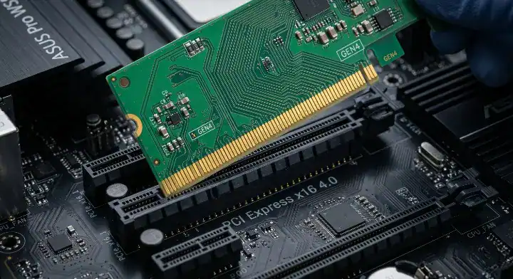
Edge connectors act as the physical bridge between peripheral cards and the main motherboard socket. You see them heavily utilized in PCI, PCIe, AGP, and ISA slots for graphics cards and memory modules. The gold layer delivers superior electrical conductivity, which means high-frequency data transfers happen without packet loss. Here are the facts regarding edge connectivity:
- Gold never tarnishes or reacts with atmospheric oxygen.
- The metal maintains a low contact resistance of less than 15 milliohms.
- Edge connectors allow for hot-swappable modular hardware designs.
Key Takeaway
Designing highly durable edge interfaces prevents sudden data transfer failures in harsh industrial environments.
Bottom line: Always specify hard gold over standard finishes for any peripheral card that plugs into a motherboard slot to prevent contact oxidation.
| Feature | Copper Pad | Gold Finger Pad | Performance Gain |
|---|---|---|---|
| Oxidation Resistance | Very Poor | Excellent | Prevents signal blocking |
| Contact Resistance | High over time | <15 milliohms | Stable data transfer |
| Insertion Cycles | <5 | 1000+ | Extended hardware lifespan |
Gold plating fundamentally solves the contact resistance degradation that naturally plagues bare copper interfaces over time.
2. How Does the Plating Process for PCB Gold Fingers Work?
The electroplating process for PCB gold fingers involves depositing 0.004 to 0.008 mil of nickel, followed immediately by 0.04 to 0.08 mil of hard gold. This sequential layering creates a robust, oxidation-resistant surface because the nickel acts as a critical diffusion barrier preventing copper migration.
The Nickel Diffusion Barrier
Without a nickel barrier layer, copper atoms actively migrate into the gold layer, completely destroying its conductivity. You must apply the nickel plating first to seal the copper traces. Look at the sequence steps:
- Boards undergo chemical cleaning to strip away surface oxides.
- An electroplating bath applies the 0.006 mil nickel layer.
- The board receives a final electroplated wash of cobalt-hardened gold.
The Cobalt Hardening Process
Pure gold is far too soft to withstand friction. Manufacturers mix 5% to 10% cobalt into the gold plating bath, which means the resulting alloy becomes structurally rigid and heavily resistant to abrasion.
Key Takeaway
The plating process determines the exact physical durability of your connection points.
Bottom line: Verify with your manufacturer that they apply a minimum of 0.004 mil nickel before the gold layer to stop copper diffusion entirely.
| Plating Layer | Thickness Specs | Primary Function |
|---|---|---|
| Base Copper | 1 oz to 2 oz | Electrical conduction |
| Nickel Barrier | 0.004 to 0.008 mil | Stops copper migration |
| Hard Gold | 0.04 to 0.08 mil | Provides wear resistance |
The structural integrity of the edge connector relies entirely on the precise thickness of the underlying nickel barrier.
3. What Are the Design Rules for PCB Gold Fingers?
Applying strict design rules for PCB gold fingers guarantees that your boards survive the abrasive edge beveling process without mechanical damage. You must maintain a minimum distance of 1.0mm between any Plated Through Hole (PTH) and the gold finger pads to prevent structural fracturing.
Beveling Angles and Thickness Rules
(1) Question: “My gold fingers keep getting damaged during edge beveling. The bevel cuts into the gold plating on boards thinner than 1.2mm. What’s the minimum board thickness for safe beveling?” (Source: SierraConnect) You must design a minimum board thickness of 1.2mm to safely bevel the edges, though 1.6mm or higher remains the safest industry standard. If a board is thinner than 1.2mm, the V-cut router blade structurally damages the gold plating. Typical bevel angles include 20°, 30°, 45°, and 60°, depending precisely on the target motherboard slot depth.
Factory DFM Adjustments
A networking client recently faced a 15% scrap rate because their design placed SMD components 0.5mm from the finger edge, causing solder mask to bleed onto the gold. We instituted a hard rule enforcing a 1.5mm clearance zone and stripped all silkscreen from the connector area. This immediate engineering adjustment dropped their scrap rate to exactly 0% across 5,000 produced boards. Consider these strict layout guidelines:
- Point all gold fingers outward toward the board edge.
- Keep standard trace widths entering the fingers at 8 mil minimum.
- Remove all solder mask and silkscreen from the finger area entirely.
Key Takeaway
Following specific mechanical clearances prevents your boards from being destroyed during the final routing stages.
Bottom line: Always design a 1.5mm keep-out zone around your edge connectors and specify a board thickness of at least 1.6mm for standard PCIe slots.
| Board Thickness | Safe Beveling? | Recommended Bevel Angle |
|---|---|---|
| 0.8mm | No (Plating damage) | N/A |
| 1.2mm | Yes (Minimum) | 45 degrees |
| 1.6mm | Yes (Standard) | 30 or 45 degrees |
Standardizing your board thickness to 1.6mm structurally eliminates the risk of bevel router blades cutting into your conductive gold pads.
4. Hard Gold vs ENIG: Which Plating Should You Choose for PCB Gold Fingers?
Choosing between Hard Gold and ENIG for PCB gold fingers depends entirely on your product’s anticipated physical mating cycles. Hard gold utilizes a cobalt alloy to achieve a thickness of 30µin to 50µin, resulting in a surface that withstands 1000+ insertions. Electroless Nickel Immersion Gold (ENIG) sits at 2µin to 5µin, failing rapidly under repeated physical friction.
Analyzing Insertion Cycle Lifespans
(2) Question: “Is ENIG good enough for gold fingers or do I always need hard gold? My board only gets plugged in 2-3 times during its lifetime.” (Source: Electronics forums) If your board experiences fewer than 10 insertion cycles during its entire lifespan, ENIG is completely acceptable and saves manufacturing costs. For hardware expecting 10 to 100 cycles, you need at least 15µin of hard gold. If the product faces over 100 insertions, you must mandate 30µin to 50µin of hard gold. ENIG’s primary failure mode under friction involves the thin gold layer wearing off, exposing the oxidizable nickel and spiking contact resistance.
Cost and Performance Balance
Hard gold electroplating requires an electrical tie-bar during manufacturing, which means the process adds distinct setup time and labor costs compared to ENIG. Review these material differences:
- Hard gold rates at 130-150 Knoop hardness.
- ENIG rates at a much softer 90 Knoop hardness.
- Hard gold struggles with fine-pitch soldering due to its thickness.
Key Takeaway
Matching your plating chemistry to your expected physical wear prevents both over-engineering and premature field failures.
Bottom line: Specify 30µin hard gold for any peripheral card that users will frequently plug and unplug, such as RAM modules or SD cards.
| Plating Type | Gold Thickness | Hardness (Knoop) | Max Safe Insertions |
|---|---|---|---|
| ENIG | 2µin – 5µin | 90 | < 10 |
| Hard Gold | 30µin – 50µin | 130 – 150 | 1000+ |
Standard ENIG chemistry provides excellent solderability for surface mount components but severely lacks the mechanical durability required for sliding contacts.
5. How Do IPC-4556 Standards Control PCB Gold Fingers Quality?
The IPC-4556 standard dictates the exact plating thicknesses and quality metrics required for PCB gold fingers to achieve certification. This framework mandates a baseline of 32µin (microinches) for high-reliability edge contacts, allowing a strict processing range strictly between 3µin and 50µin based on the application class.
Enforcing Thickness Metrics
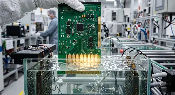
Operating below IPC standards results in premature wear, while exceeding 50µin causes the gold to become excessively brittle. Factories utilize X-ray fluorescence (XRF) machines to measure this microscopic thickness precisely. Observe the IPC verification rules:
- Class 1 products allow thinner 15µin plating.
- Class 3 aerospace products mandate 32µin minimum.
- Visual inspections must verify zero pitting or nodules.
Chemical Purity Requirements
The IPC-4556 standard also dictates the purity of the chemical bath. The gold deposit must maintain a minimum 99.7% purity level, heavily regulating the cobalt hardener ratio to prevent signal attenuation.
Key Takeaway
Adhering to IPC-4556 guarantees your edge connectors survive aggressive environmental testing and long-term mechanical friction.
Bottom line: Always request an XRF thickness report from your manufacturer to verify that your gold plating strictly meets the IPC-4556 32µin requirement.
| IPC Class | Application | Min Gold Thickness | Quality Check |
|---|---|---|---|
| Class 1 | Consumer toys | 15µin | Visual |
| Class 2 | Standard IT gear | 30µin | XRF scan |
| Class 3 | Medical / Aerospace | 32µin – 50µin | XRF + Tape test |
Stringent IPC classification testing ensures that critical medical and aerospace edge connectors never fail during active physical operation.
6. What Are the Exact Costs Associated with PCB Gold Fingers?

Adding PCB gold fingers to your bare board fabrication increases the per-unit cost significantly due to the soaring market price of raw gold salts and extra processing steps. Hard gold plating typically adds $0.50 to $2.00 per board depending directly on the total calculated surface area of the edge contacts.
Area and Thickness Calculations
Because electroplating charges scale linearly with material usage, asking for 50µin of gold costs nearly double what 30µin costs. Here are the primary cost drivers:
- Total square inches of the finger pads.
- The designated thickness requirement (e.g., 30µin vs 15µin).
- The manual labor required to tape off the rest of the board.
Panel Utilization Economics
Factories must attach temporary electrical tie-bars to the panel edges to conduct current during electroplating. This requirement consumes valuable panel real estate, which means you get fewer usable boards out of a standard 18×24 inch production panel.
Key Takeaway
Optimizing your finger pad dimensions prevents you from paying for expensive precious metals that your motherboard slot doesn’t actually contact.
Bottom line: Reduce your edge connector length to match only the exact depth of the mating slot to cut your gold plating costs by up to 20%.
| Cost Driver | Variable | Price Impact |
|---|---|---|
| Gold Thickness | 15µin vs 30µin | High ($$) |
| Surface Area | Connector length/width | High ($$) |
| Panel Space | Tie-bar routing limits | Medium ($) |
Controlling the physical dimensions and thickness specifications of your edge contacts is the fastest way to lower your bare board manufacturing costs.
7. What Are Common PCB Gold Fingers Manufacturing Defects and How to Prevent Them?
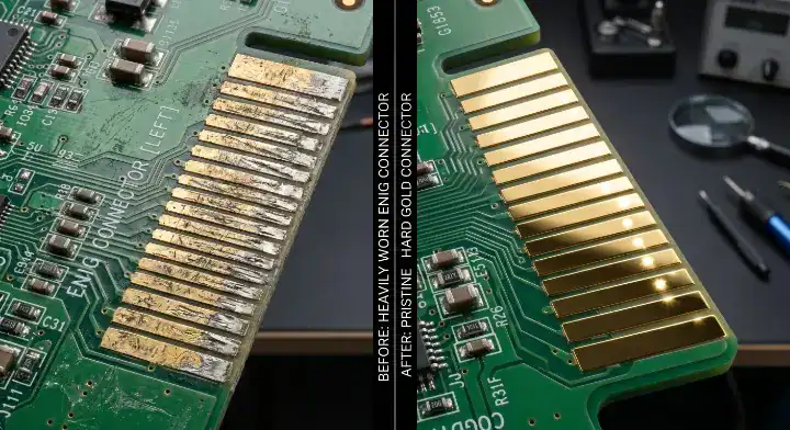
Identifying manufacturing defects in PCB gold fingers early prevents massive field failures caused by peeling plating or corroded nickel. Common critical defects include insufficient adhesion, uneven gold distribution across the pins, and mechanical scratches inflicted during the edge beveling sequence.
Solving Plating Adhesion Failures
(3) Question: “We received a batch of PCBs where the gold finger plating is peeling off after a few insertion cycles. What went wrong in the plating process?” (Source: PCB质量问题讨论) Insufficient adhesion directly occurs when the nickel layer is too thin or the copper surface lacks proper chemical cleaning before plating. You must enforce the ASTM B571 tape test on every batch to verify adhesion strength. Furthermore, if the cobalt hardener ratio drops below 5%, the gold lacks friction resistance; if it exceeds 10%, the plating becomes dangerously brittle and flakes off.
Resolving Uneven Current Distribution
A server motherboard client suffered from uneven gold layers, where the outer pins had 40µin but the center pins only had 15µin. We redesigned their electroplating tie-bars to balance the cathode current density evenly across the entire edge. This immediate factory adjustment stabilized the thickness deviation to under 2µin, achieving 100% IPC compliance. Review these defect prevention methods:
- Verify plating bath chemistry daily.
- Use specialized plating tape to prevent chemical bleed.
- Monitor current density to prevent nodule formation.
Key Takeaway
Rigorous physical testing catches weak plating bonds before the hardware ever ships to your end customer.
Bottom line: Mandate that your fabrication partner performs and passes the ASTM B571 tape test on a sample board from every production lot.
| Common Defect | Root Cause | Factory Prevention Method |
|---|---|---|
| Peeling Plating | Poor copper cleaning | ASTM B571 Tape Test |
| Uneven Thickness | Bad current distribution | Redesign plating tie-bars |
| Brittle Flaking | >10% Cobalt ratio | Daily bath chemistry checks |
Maintaining absolute chemical purity in the electroplating tanks physically prevents the formation of brittle structures inside the gold alloy.
8. Why Is Inner Layer Copper Removal Required for PCB Gold Fingers?
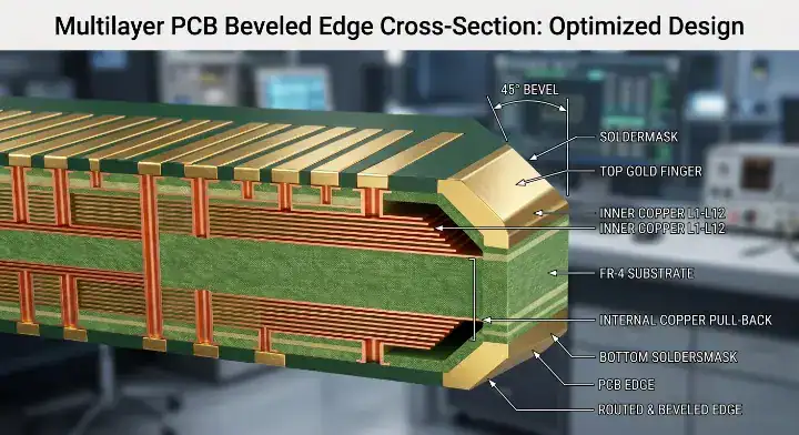
Removing inner layer copper beneath PCB gold fingers physically prevents catastrophic short circuits from occurring during the 45-degree edge beveling process. If inner copper planes extend to the very edge of the board, the V-cut router blade cuts through them, exposing raw copper on the sloped edge.
Preventing Electrical Shorts
When you insert a beveled edge with exposed inner copper into a tight slot, the motherboard socket pins can easily bridge the exposed layers. Pulling back the internal copper planes by at least 1.0mm creates a safe margin of solid FR-4 fiberglass. Consider these routing facts:
- Exposed inner copper oxidizes and creates conductive dust.
- Beveling blades drag copper smears across the board edge.
- Solid FR-4 edges provide safer, smoother insertion friction.
Managing Impedance Mismatch
Removing copper planes directly underneath the finger pads creates a sudden change in dielectric distance, resulting in severe impedance mismatch for high-speed PCIe signals. Engineers must recalculate the trace widths precisely at the edge connector zone to maintain the target 85-ohm or 100-ohm differential impedance.
Key Takeaway
Proper copper pullback rules protect your multi-layer boards from shorting out inside expensive motherboard sockets.
Bottom line: Instruct your layout engineers to clear all inner layer ground and power planes at least 1.0mm away from the beveled edge of the connector.
| Design Element | Distance from Edge | Reason for Rule |
|---|---|---|
| Hard Gold Pad | 0.0mm (On edge) | Mating contact |
| Inner Copper Plane | > 1.0mm pullback | Prevents bevel shorting |
| Plated Through Hole | > 1.0mm clearance | Prevents structural cracking |
Clearing internal copper from the bevel zone is a mandatory mechanical requirement for any circuit board thicker than two layers.
9. How Do You Panelize Boards with PCB Gold Fingers for Assembly?
Panelizing boards featuring PCB gold fingers requires specialized routing patterns because the edge connectors must permanently face outward to connect to the electroplating bus bar. You cannot place two edge connectors facing inward toward each other inside the panel frame.
Plating Tie-Bar Requirements
During fabrication, all gold pads must maintain a continuous electrical connection to conduct the electroplating current. Factories achieve this by extending copper traces off the board edge into a sacrificial tie-bar on the panel frame, which means the fingers must be positioned on the outer perimeter. Look at the panelization strategies:
- Orient all edge connectors facing the panel rails.
- Use mouse bites (breakaway tabs) on non-connector edges.
- Maintain a 10mm handling border around the panel.
Post-Assembly Routing
After the surface mount assembly process finishes, the factory removes the sacrificial tie-bar using a precise V-cut or CNC router. The router must chamfer the edge simultaneously to create the final 45-degree mating slope.
Key Takeaway
Planning your panel layout around the electroplating bus bar drastically reduces material waste and lowers manufacturing costs.
Bottom line: Never place gold finger edges facing each other inside an array; always orient them outward toward the sacrificial panel rails.
| Panel Layout Factor | Best Practice | Impact on Production |
|---|---|---|
| Finger Orientation | Facing outward | Enables electroplating |
| Breakaway Tabs | On side/top edges | Prevents finger damage |
| Array Spacing | 2mm between boards | Allows clean routing |
Correctly orienting your edge connectors inside the production array is fundamentally necessary to establish the electrical circuit required for hard gold plating.
10. When Should You Avoid Using PCB Gold Fingers in Your Design?
You should actively avoid designing PCB gold fingers if your product requires extreme vibration resistance or handles lethal high-voltage currents. While edge connectors provide excellent modularity, they suffer from mechanical micro-fretting in high-vibration aerospace environments, resulting in intermittent signal drops.
Evaluating Alternative Connectors
If a board requires a permanent, high-current connection, standard through-hole header pins or locking wire-to-board connectors outperform edge contacts significantly. Review these avoidance scenarios:
- Industrial robotics experiencing constant mechanical shock.
- High-voltage power supplies exceeding 100V.
- Sealed waterproof devices where edge slots create leak points.
The ENIG Exception for Low Use
If your device utilizes a programming debug port that engineers only plug into once during initial factory calibration, paying for a hard gold bevel is a waste of capital. Utilizing the standard ENIG surface finish provides perfect connectivity for a single-use insertion at zero extra cost.
Key Takeaway
Understanding the mechanical limitations of edge slots allows you to select far more reliable locking connectors for harsh environments.
Bottom line: Switch to mechanical locking headers instead of edge connectors if your hardware will operate in high-vibration automotive or aerospace conditions.
| Connection Type | Vibration Resistance | Best Use Case |
|---|---|---|
| Gold Edge Connector | Low | Swappable PC cards |
| Locking Header | High | Automotive / Robotics |
| Standard ENIG Edge | Low | Factory debug ports (1-2 uses) |
Locking wire-to-board connectors physically clamp down on pins, completely eliminating the micro-fretting issues associated with sliding edge sockets in vibrating machinery.
When your peripheral devices fail in the field due to worn-out edge contacts, you lose both revenue and customer trust. Perfecting your edge connector design ensures that your hardware survives thousands of physical mating cycles without signal degradation. If you need highly reliable, IPC-4556 compliant circuit boards manufactured with exact hard gold thickness tolerances, contact us today to utilize our advanced electroplating and precision beveling lines.
FAQ
Can I use ENIG instead of hard gold for my edge connectors? Yes, but only if your board will be inserted into a slot fewer than 10 times during its entire lifecycle. ENIG is too soft and thin (2-5µin) to withstand repeated friction, so you must upgrade to hard gold for high-use modules like RAM or PCIe cards. Contact our team to analyze your specific wear requirements.
What is the minimum board thickness required for edge beveling? You must use a minimum board thickness of 1.2mm, though 1.6mm is the safest industry standard. If your board is thinner than 1.2mm, the V-cut router blade will tear into the gold plating and destroy the pads. Let our DFM engineers review your stack-up before production.
How do I prevent the gold plating from peeling off my boards? You mandate that your manufacturer performs the ASTM B571 tape test on every batch. Peeling is caused by poor copper cleaning or an insufficient nickel barrier layer (under 0.004 mil). Reach out to us to experience our zero-defect plating quality control protocols.
Does adding gold edge contacts increase my PCB manufacturing time? Yes, electroplating hard gold adds approximately 1 to 2 days to your standard bare board fabrication lead time. The process requires custom taping, specific panel routing for electrical tie-bars, and secondary chemical baths. Partner with us for rapid prototyping to minimize these delays.
Why do I need to remove inner layer copper near the edge connector? Removing the inner copper planes prevents catastrophic short circuits during the beveling process. If the 45-degree router blade cuts through internal copper, it exposes the metal, which can easily short out the pins inside your motherboard socket. Submit your Gerber files today for a complete engineering design review.
Upload your files today · Free DFM check before production · Ship worldwide
Get your PCB prototypes in as fast as 24 hours. We handle FR4, Rogers, and Flex up to 60 layers — free prototypes for 2–4 layer boards, no minimum order.
Just upload your Gerber + BOM — we source every part, assemble, and inspect (AOI + X‑Ray) so you don't have to chase suppliers. Boards ship in as fast as 24 hours.