
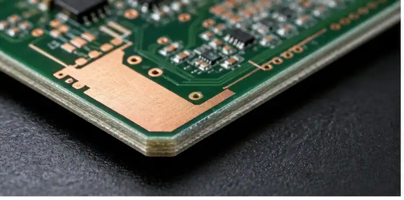
Quick Answer: Decision: copper-to-edge review. Controlled object: marked outer and inner copper views aligned to the finished routed and V-score outline. Design-owned boundary: intentional edge contacts, antenna keepouts, high-voltage spacing, and the approved finished profile. Supplier discretion: routine routing compensation that preserves the released keepout and does not remove functional copper. Stop rule: a score line crossing copper, a route-to-plane conflict, or an unlabeled feature intentionally reaching the edge.
Copper edge RFQ path
- Why does copper-to-edge clearance affect RFQ risk?
- Which copper features should be checked?
- How do routing and V-score change clearance?
- Which DFM fixes need design approval?
- How should buyers compare supplier answers?
- What should a copper-edge RFQ package include?
Why does copper-to-edge clearance affect RFQ risk?
PCB copper-to-edge clearance requirements affect RFQ risk because routing, scoring, depaneling, plating, and handling can expose or damage copper near the finished board edge. The buyer should treat edge copper as a process and acceptance issue, not only as a layout DRC value.
- Copper near routed edges can be nicked, exposed, or weakened during profiling.
- V-score edges often need more clearance than routed edges.
- Functional edge copper needs a special approval path instead of silent CAM cleanup.
| Edge condition | Buyer decision |
|---|---|
| Normal routed outline | Use supplier standard clearance unless fit is tight |
| V-score separation | Review larger clearance and break edge condition |
| Copper intentionally at edge | Treat as a controlled special feature |
Bottom line: Edge clearance protects both manufacturability and the buyer’s acceptance standard.
Which copper features should be checked?
The RFQ should check traces, planes, pads, vias, shields, castellations, plated edges, test pads, and copper pours near the finished outline. Each feature has a different reason for being close to the edge, so one global answer can create the wrong manufacturing decision.
- Separate accidental copper pour near the outline from intentional edge contacts.
- Review inner-layer copper near routed or scored edges, not just visible outer copper.
- Identify high-voltage, RF, antenna, or connector areas before approving changes.
| Feature near edge | Review reason |
|---|---|
| Trace or plane | Risk of exposure or reduced clearance |
| Pad or via | Risk of breakout or solderability change |
| Plated edge / castellation | Special process rather than normal clearance |
Bottom line: The supplier needs to know whether near-edge copper is accidental, functional, or prohibited.
How do routing and V-score change clearance?
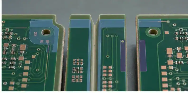
Routing and V-score change clearance because the edge is formed differently. A routed edge follows a cutter path and can handle more complex shapes, while a scored edge creates a break line that may require more distance from copper on all layers. The RFQ should state which edge method is allowed.
- Do not apply a routed-edge assumption to a scored panel without review.
- Check panel tabs and mouse bites when copper sits near a breakaway area.
- Ask for CAM feedback when edge copper is close to an internal cutout or slot.
| Method | Clearance concern |
|---|---|
| CNC routing | Router path, burr, and tool wander |
| V-score | Break stress and exposed copper risk |
| Tab routing | Residue and local edge damage near copper |
Bottom line: Clearance cannot be separated from the chosen depaneling method.
Which DFM fixes need design approval?
DFM fixes need design approval when they move copper, trim planes, change impedance areas, alter RF/antenna behavior, affect high-voltage clearance, or remove intentional edge contacts. Simple copper-pour pullback may be easy, but the supplier should not decide functional copper changes alone.
- Ask whether the proposed pullback is local, layer-specific, or global.
- Check RF, shield, connector, and high-voltage regions before approving copper movement.
- Keep approved clearance exceptions with the released fabrication files.
| DFM fix | Approval concern |
|---|---|
| Plane pullback | May affect shielding or impedance environment |
| Trace reroute | May change timing, clearance, or EMI behavior |
| Exception accepted | Needs inspection and acceptance wording |
Bottom line: Pulling copper back is only safe when it does not change the circuit intent.
How should buyers compare supplier answers?
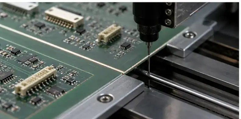
Buyers should compare supplier answers by edge method, minimum clearance assumption, layers affected, DFM authority, evidence offered, and how exceptions are handled. One supplier may quote faster by assuming standard pullback, while another may hold production until engineering approves near-edge copper.
- Ask suppliers to state whether they will modify copper during CAM.
- Compare clearance requirements separately for routing, scoring, and tab areas.
- Treat no-warning quotes carefully when the design has intentional edge copper.
| Supplier answer | Buyer interpretation |
|---|---|
| Standard pullback allowed | Fast but needs design-owner permission |
| Hold for approval | Safer for functional edge copper |
| No exception review | Risky for plated-edge or RF designs |
Bottom line: Quote comparison should include the accepted copper-edge assumption, not just price.
What should a copper-edge RFQ package include?
A copper-edge RFQ package should include the outline layer, copper layers, panel method, edge-processing notes, intentional edge-copper locations, allowed CAM pullback rule, and evidence request. That gives QueenEMS enough information to separate normal DFM cleanup from product-level changes.
- Mark intentional edge copper and prohibited pullback zones.
- State whether routing, V-score, or tab routing is acceptable.
- Request evidence only where edge condition affects acceptance or reliability.
| RFQ item | Purpose |
|---|---|
| Edge method | Sets the clearance rule |
| Copper exception map | Protects functional near-edge copper |
| Inspection request | Documents exposed-copper or edge-damage risk |
Bottom line: The RFQ should make near-edge copper intentional, removable, or forbidden.
What should the buyer record before release?
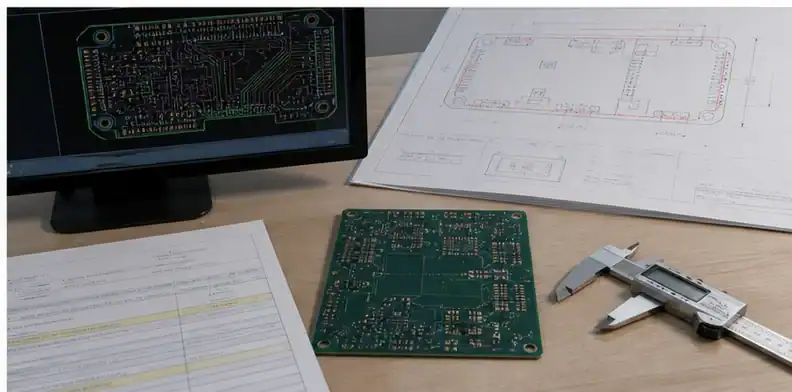
Production record for the copper-to-edge review
Controlled object
Controlled object: marked outer and inner copper views aligned to the finished routed and V-score outline.
Failure boundary
Failure boundary: exposed copper, weakened dielectric margin, scoring damage, or an unintended chassis contact.
Design-owned conditions
Design-owned conditions: intentional edge contacts, antenna keepouts, high-voltage spacing, and the approved finished profile.
Supplier discretion
Supplier discretion: routine routing compensation that preserves the released keepout and does not remove functional copper.
Required proof
Required proof: a processed CAM view for every exceptional edge zone plus the first-article edge condition when acceptance depends on appearance.
Production stop
Production stop: a score line crossing copper, a route-to-plane conflict, or an unlabeled feature intentionally reaching the edge.
Repeat-order baseline
Repeat-order baseline: the outline revision, edge process, accepted exception map, and receiving evidence for the approved lot.
RFQ inputs
RFQ inputs: Gerber or ODB++, drill data, fabrication drawing, panel method, copper weights, edge-contact notes, quantity, and acceptance rule.
FAQ
Can the supplier decide the copper-to-edge review?
Discretion for copper-to-edge review: routine routing compensation that preserves the released keepout and does not remove functional copper. Engineering control for copper-to-edge review: intentional edge contacts, antenna keepouts, high-voltage spacing, and the approved finished profile.
What stops this copper-to-edge review?
Stop rule for copper-to-edge review: a score line crossing copper, a route-to-plane conflict, or an unlabeled feature intentionally reaching the edge. Disposition owner for copper-to-edge review: the named engineering approver.
Which proof closes the copper-to-edge review?
Evidence for copper-to-edge review: a processed CAM view for every exceptional edge zone plus the first-article edge condition when acceptance depends on appearance. Revision link for copper-to-edge review: the quoted dataset.
What survives into the next order?
Reorder baseline for copper-to-edge review: the outline revision, edge process, accepted exception map, and receiving evidence for the approved lot.
For a focused copper-to-edge review, send QueenEMS Gerber or ODB++, drill data, fabrication drawing, panel method, copper weights, edge-contact notes, quantity, and acceptance rule. Redline request: copper-to-edge review. Open assumptions: copper-to-edge review. Approver: copper-to-edge review owner.
Written by the QueenEMS Engineering Team
Sources
Upload your files today · Free DFM check before production · Ship worldwide
Get your PCB prototypes in as fast as 24 hours. We handle FR4, Rogers, and Flex up to 60 layers — free prototypes for 2–4 layer boards, no minimum order.
Just upload your Gerber + BOM — we source every part, assemble, and inspect (AOI + X‑Ray) so you don't have to chase suppliers. Boards ship in as fast as 24 hours.