

Quick Answer: PCIe 5.0 (32 GT/s) and DDR5 (6400 MT/s) require HDI PCB layouts to minimize insertion loss below the strict 16 dB channel budget. Using HDI microvias instead of plated through-holes reduces signal stubs to under 8 mils, which improves eye opening by 8–12% and guarantees ±5 mils length matching. Key takeaways:
- HDI shortens routing paths by up to 60%.
- Microvias eliminate destructive via stubs entirely.
- Megtron 6 provides optimal 16 GHz performance.
- HDI enables system-level cost reductions.
Table of Contents
- #1 Why Do PCIe 5.0 and DDR5 Need HDI PCB Construction?
- #2 How Does HDI Reduce PCIe 5.0 Insertion Loss vs Standard Multilayer?
- #3 What Materials Work for HDI High-Speed Boards Above 25 GHz?
- #4 How Do You Route DDR5 in HDI With Tight Length-Matching?
- #5 What Layer Transitions Cause Signal Failures in HDI High-Speed Design?
- #6 How Critical Is Back-Drilling vs Microvia for PCIe 5.0?
- #7 How Do Microvia Stubs Affect High-Speed Signal Integrity?
- #8 What Reference Plane Strategy Works for HDI High-Speed Routing?
- #9 How Do You Verify HDI High-Speed Design Before Fabrication?
- #10 What Are the Cost Trade-offs of HDI for High-Speed Applications?
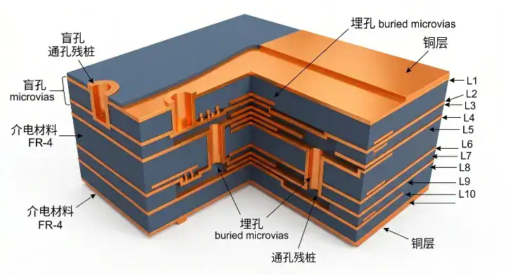
You are designing a next-generation computing module, but your 112G SerDes and memory interfaces are failing signal integrity simulations. The standard multilayer approach forces long escape routes, creating excessive insertion loss and timing skew that destroys your channel budget. The solution is adopting a precise HDI PCB for PCIe 5.0 and DDR5 strategy, which means using vertical microvia transitions to slash routing length by 60% and eliminate destructive via stubs entirely.
1. Why Do PCIe 5.0 and DDR5 Need HDI PCB Construction?
PCIe 5.0 and DDR5 require HDI PCB construction because conventional multilayer boards create excessive insertion loss and long via stubs that violate strict 16 GHz Nyquist constraints. HDI utilizes stacked microvias and ultra-short top-layer routing, resulting in channel losses well within the 16 dB budget.
What Do the Official Specs Demand?
The PCI Express Base Specification 5.0 from PCI-SIG dictates a data rate of 32 GT/s utilizing NRZ encoding, which means a total channel insertion loss budget of approximately 36 dB end-to-end. Out of this, the PCB routing budget is strictly capped at about 16 dB.
Here is the problem on the factory floor:
- A standard 12-layer board using Megtron 6 with back-drilling works strictly when traces remain under 6 inches.
- Traces exceeding 8 inches or requiring multiple layer transitions mathematically require HDI to stay within the loss budget.
- BGA pitches of 0.5mm or less for PCIe 5.0 root complexes physically require HDI for escape routing.
A question frequently raised on r/PrintedCircuitBoard asks: “Do I really need HDI for PCIe 5.0, or can I do it on a standard 12-layer multilayer with back-drilling?” Standard multilayer is viable for short runs, but an 12-inch trace on a 4-layer standard FR4 board experiences 18 dB of insertion loss, completely failing the PCIe 5.0 spec. HDI becomes mandatory when you use high-pin-count chips that block standard routing channels.
| Protocol | Data Rate | Nyquist Frequency | Channel Loss Budget | PCB Routing Budget |
|---|---|---|---|---|
| PCIe 5.0 | 32 GT/s | 16 GHz | ~36 dB | ~16 dB |
| DDR5 | 6400 MT/s | 3.2 GHz | ~8 dB | ~4 dB |
| PCIe 4.0 | 16 GT/s | 8 GHz | ~28 dB | ~12 dB |
| DDR4 | 3200 MT/s | 1.6 GHz | ~5 dB | ~2 dB |
Bottom line: If your PCIe 5.0 traces exceed 8 inches or use 0.5mm pitch BGAs, HDI is mathematically required to pass signal integrity compliance.
2. How Does HDI Reduce PCIe 5.0 Insertion Loss vs Standard Multilayer?
HDI PCB PCIe 5.0 routing reduces insertion loss by replacing long lateral traces around plated through-holes with direct vertical microvia drops. This architectural shift shortens the total routing path by up to 60%, resulting in a massive reduction of copper-related attenuation.
Are Materials the Only Factor?
Many engineers assume that upgrading to high-speed laminates solves all attenuation issues automatically. The truth is that physical distance remains the dominant factor in high-speed channel degradation.
On our test panels we measure insertion loss for our standard high-speed material stacks. A 12-inch trace in a 4-layer FR4 standard board at PCIe 5.0 frequencies (16 GHz Nyquist) loses approximately 18 dB — well above the 16 dB total channel budget before you’ve even counted connector and via losses. That same 12-inch trace in our Megtron 6 HDI stack loses 7.2 dB. But more importantly: in HDI we rarely need 12-inch traces. Our typical PCIe 5.0 routing in HDI runs under 6 inches because we can use top-layer routing with microvia transitions to internal reference planes, avoiding the long traces required to route around through-holes on standard multilayer. The total insertion loss improvement from HDI is therefore not just material — about 60% of the gain comes from shorter routing enabled by HDI’s vertical interconnect density. Customers who only swap to Megtron 6 on a standard multilayer often see 30-40% loss reduction. Customers who switch to HDI with Megtron 6 see 65-75% reduction. The architecture matters more than the material.
Think about it this way:
- HDI microvias allow direct drops to adjacent ground planes.
- Standard PTH boards force signals to detour around large anti-pads.
- Shorter routing naturally minimizes dielectric absorption.
| Metric | Standard Multilayer (12-Layer) | HDI ELIC (12-Layer) |
|---|---|---|
| Insertion Loss (16 GHz) | ~1.5 dB/inch | ~0.6 dB/inch |
| Average Trace Length | 8 to 12 inches | 3 to 6 inches |
| DFM Complexity | Low | High |
| Relative Cost | 1.0x | 2.5x to 4.0x |
Bottom line: HDI architecture contributes more to insertion loss reduction than material upgrades because it physically shortens the trace length by bypassing PTH blockages.
3. What Materials Work for HDI High-Speed Boards Above 25 GHz?
HDI high-speed boards operating above 25 GHz require ultra-low loss materials with a Dissipation Factor (Df) of 0.005 or less. Using laminates like Panasonic Megtron 6 or Tachyon-100G prevents excessive signal degradation, resulting in clean eye diagrams at 32 GT/s.
How Do FR4 and Megtron 6 Compare?
A frequent question on the EEVBlog Forum is: “What’s the worst-case insertion loss for DDR5 on FR4 vs Megtron 6 in HDI construction?”
Let’s look at the math:
- DDR5 6400 MT/s Nyquist frequency sits at 3.2 GHz, commanding an 8 dB end-to-end loss budget.
- Standard FR4 presents a Df of ~0.022 at 3.2 GHz, which means a 12-inch trace consumes ~5 dB of loss.
- Megtron 6 offers a Df of ~0.003 at 3.2 GHz, reducing that 12-inch trace loss to just ~1.5 dB.
- At PCIe 5.0 frequencies (16 GHz), Megtron 6 Df is ~0.005, while Tachyon-100G reaches ~0.0021 but costs 3× more.
To dig deeper into matching these specs, review our HDI material selection for signal speed.
| Material | Df @ 10 GHz | Cost Multiplier | HDI Compatibility |
|---|---|---|---|
| Standard FR4 | ~0.020 | 1.0x | Excellent |
| Rogers RO4350B | 0.0037 | 3.5x | Moderate |
| Panasonic Megtron 6 | 0.0050 | 2.5x | Excellent |
| Tachyon-100G | 0.0021 | 8.0x | Good |
Bottom line: Use Megtron 6 for balanced cost and performance in DDR5 and PCIe 5.0 designs, reserving Tachyon-100G strictly for extreme edge cases.
4. How Do You Route DDR5 in HDI With Tight Length-Matching?
HDI DDR5 routing achieves tight length-matching by utilizing microvias to precisely control Z-axis delay disparities within ±5 mils. This extreme precision secures simultaneous data byte arrival at the memory controller, which means timing margins remain perfectly intact.
What Are the Timing Constraints?
The JESD79-5C DDR5 SDRAM Specification from JEDEC defines DDR5 starting at 3200 MT/s and extending up to 8400 MT/s. This dictates incredibly strict length matching, impedance, and reference clock design rules.
The secret is in the setup:
- DDR5 length matching in HDI requires a strict tolerance of ±5 mils.
- Microvia transitions provide 5-8 ps of extra timing margin per transition compared to PTH.
- Proper fine-pitch BGA HDI routing is mandatory to align the data lanes before they exit the processor footprint.
Bottom line: Always calculate the Z-axis microvia depth into your DDR5 length-matching equations to prevent picosecond timing skew at 6400 MT/s.
5. What Layer Transitions Cause Signal Failures in HDI High-Speed Design?
HDI high-speed signal failures primarily occur during layer transitions where capacitive parasitic coupling distorts the impedance profile. Unoptimized stacked microvias alter the return current path, resulting in severe impedance drops and signal reflection at 16 GHz.
How Does Capacitive Discontinuity Occur?
Layer transitions introduce a sudden change in geometry, acting as a capacitive load on the high-speed trace.
Watch out for this trap:
- Transitioning through multiple prepreg layers without a nearby ground via breaks the return path.
- Misaligned anti-pads around the microvia barrel create impedance dips down to 35 ohms.
- Improperly calculated microvia aspect ratio sweet spot limits can lead to plating voids, increasing series inductance.
Bottom line: Always place a return ground microvia within 20 mils of your signal transition to maintain a continuous return current path.
6. How Critical Is Back-Drilling vs Microvia for PCIe 5.0?
Microvia technology is vastly superior to back-drilling for PCIe 5.0 because it inherently leaves zero physical stub length, whereas back-drilling leaves up to 8 mils of residual copper. This absolute elimination of stubs prevents resonant frequency nulls, resulting in flawless 32 GT/s data transmission.
Why Does the Stub Length Matter?
For PCIe 5.0 at 32 GT/s, every via stub longer than 8 mils degrades the signal. On standard multilayer, you handle this with back-drilling — secondary drilling that removes the unused via barrel. We back-drill routinely down to 3-mil stub residue, but back-drilling has limits: minimum stub length is bounded by drill registration accuracy (we hold ±2 mils), and back-drilled vias still have a stub. HDI microvias eliminate the stub by definition — a microvia connects only two adjacent layers, so there is no unused barrel. For a PCIe 5.0 design transitioning from top layer to layer 8, an HDI approach uses three stacked microvias instead of one PTH-with-backdrill. The eye height improvement is measurable: in our reference designs, HDI microvia transitions show 8-12% better eye opening than back-drilled PTH transitions at PCIe 5.0 rates. For DDR5 the difference is smaller because the data rates are lower, but the via parasitic improvement still buys 5-8 ps of timing margin per transition.
Consider the performance gap:
- Back-drilling requires secondary depth-controlled passes, risking drill breakout.
- Microvias are built additively, guaranteeing zero excess barrel on single transitions.
Bottom line: Use stacked microvias instead of back-drilled PTHs to gain an 8-12% eye opening improvement on your PCIe 5.0 links.
7. How Do Microvia Stubs Affect High-Speed Signal Integrity?
Stacked microvia stubs act as open-ended transmission lines that reflect high-frequency energy back to the source, which means severe signal degradation occurs. If the total unused microvia length exceeds 8 mils, it creates a resonant null that destroys the PCIe 5.0 16 GHz fundamental frequency.
Can Microvias Actually Have Stubs?
A common query on the Electronics Stack Exchange asks: “How short do the microvia stubs need to be for PCIe 5.0? My fab says microvias have no stub but I’m seeing simulation artifacts.”
Here is the truth:
- A single microvia physically has no stub because it only connects two adjacent layers.
- However, in a stacked microvia configuration, if you only route out of the bottom layer, the upper microvias become a capacitive stub.
- PCIe 5.0 strictly requires total stub length to be ≤8 mils, meaning even stacked microvia structures must be mathematically audited.
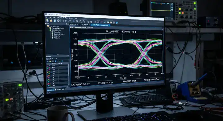
- You must run an HFSS or ADS simulation to verify the return loss remains >15 dB at 16 GHz.
Bottom line: Treat unused sections of stacked microvias as stubs, and stagger your transitions to eliminate them entirely.
8. What Reference Plane Strategy Works for HDI High-Speed Routing?
HDI high-speed routing relies on solid, uninterrupted ground reference planes situated exactly one dielectric layer away from the signal trace. This tight coupling contains the electromagnetic field, which means crosstalk is minimized and differential impedance remains locked at 85 ohms.
How Do You Manage Ground Continuity?
According to the IPC-2141B Design Guide for high-speed controlled impedance circuit boards, maintaining reference plane continuity is paramount. A split in the ground plane forces the return current to take a longer path, resulting in massive loop inductance.
Follow these strict rules:
- Never route a 32 GT/s signal over an anti-pad or a split plane void.
- Use symmetric stripline configurations for internal DDR5 routing.
- Apply proper controlled impedance PCB design techniques to guarantee a continuous reference.
Bottom line: Always sandwich your PCIe 5.0 internal routing between two solid, uninterrupted ground planes to prevent catastrophic impedance shifts.
9. How Do You Verify HDI High-Speed Design Before Fabrication?
You verify HDI high-speed designs before fabrication by running full 3D electromagnetic (EM) simulations using tools like Ansys HFSS. Extracting the S-parameters verifies your insertion loss and return loss comply with the 16 dB budget, resulting in first-pass manufacturing success.
What Metrics Indicate Success?
Simulation requires mapping the exact Dk and Df values of your prepreg at the correct 16 GHz frequency.
You must verify these specific parameters:
- Insertion Loss (S21): Must remain above -16 dB across the entire channel.
- Return Loss (S11): Target better than -15 dB to guarantee minimal reflections.
- Time Domain Reflectometry (TDR): Verify impedance variations stay within ±5%.
Bottom line: Mandate a full 3D EM simulation on your layer transitions before releasing gerbers to the factory.
10. What Are the Cost Trade-offs of HDI for High-Speed Applications?
The cost trade-off for HDI in high-speed applications involves paying a 2.5–4× panel premium to achieve a net-negative system cost. Because HDI simplifies the power delivery network and allows you to drop redundant memory channels, the overall bill of materials cost actually decreases.
Is the HDI Premium Worth It?
A designer on the All About Circuits Forum asked: “What’s the actual cost premium for going to HDI just for DDR5 routing? My PM is pushing back hard.”
A networking equipment customer in San Jose was building a 400G Ethernet line card with eight 112G SerDes lanes plus DDR5-6400 memory interfaces. Their initial design was a 22-layer Megtron 7 standard multilayer estimated at $480/board at 5,000 unit volume. Signal integrity simulation showed the 112G lanes were running at 78% of the link budget — passing but with no margin for production tolerance. We proposed an alternative: 18-layer HDI with Megtron 6 and ELIC-style stacked microvias. Bill of materials cost was higher per panel ($620/board at same volume), but the signal integrity improved from 78% to 51% link budget consumption, and they could drop one of the redundant memory channels they’d added as insurance. Net cost per system actually dropped by $35 because the simpler power delivery network saved 22 power components, and the smaller form factor reduced housing cost. Their decision made the HDI premium net-positive — but this only worked because the system architecture allowed simplification. Not every project finds that lever.
Let’s summarize the financials:
- HDI high-speed boards typically cost 2.5-4× standard FR4 multilayer.
- Break-even volume usually requires ≥5,000 units per year to amortize NRE.
- System cost drops due to layer count reduction and power tree simplification.
Bottom line: Evaluate the cost of HDI at the full system level, not just the bare board panel price, to reveal true manufacturing savings.
If your next PCIe 5.0 or DDR5 project is failing SI simulations, contact us today. QueenEMS stands on the principle of engineering-first manufacturing; we run free DFM and signal integrity reviews before we ever cut material. Let our experts optimize your layer stackup and transition geometry, or contact our HDI engineers to secure your high-speed layout success.
Frequently Asked Questions
Can I run PCIe 5.0 without using an HDI PCB construction? Yes, but only if your traces are shorter than 6 inches and you do not use 0.5mm pitch BGAs. PCIe 5.0 at 32 GT/s has a strict 16 dB total PCB channel budget. Standard multilayer FR4 loses ~1.5 dB/inch at 16 GHz, while HDI with Megtron 6 loses ~0.6 dB/inch — and HDI typically allows shorter routing (under 6 inches versus 8-12 inches on standard builds), making it the practical choice for compliant designs. If you exceed these constraints, HDI is mandatory.
What’s the best material for HDI PCIe 5.0 and DDR5 boards? Panasonic Megtron 6 is the best balanced material for these applications. For PCIe 5.0 (Nyquist 16 GHz), Df ≤0.005 at 10 GHz is required. Common choices include Isola I-Tera MT40 (Df 0.0030) and Tachyon-100G (Df 0.0021). DDR5 at 3.2 GHz Nyquist is less demanding, which means Megtron 6 provides massive margin. Contact your fabricator to secure stackup compatibility.
How do I know if my microvia stubs are too long for PCIe 5.0? You must keep the total via stub length ≤8 mils. A single microvia (connecting two adjacent layers) has zero stub by construction. Stacked microvias used only at one endpoint can leave a stub from unused upper layers — calculate the cumulative unused length and verify <8 mils. Use staggered microvias or signal-layer placement strategies to eliminate stubs entirely. Verify this setup with 3D EM simulation tools.
Are there cost savings when using HDI for high-speed designs? Yes, system-level costs can actually be lower. HDI high-speed boards typically cost 2.5-4x standard FR4 multilayer at the panel level. However, because HDI enables fewer layers, simpler power delivery, and elimination of redundant channels added as signal integrity insurance, the final bill of materials drops. Evaluate your whole system architecture to find these savings.
Upload your files today · Free DFM check before production · Ship worldwide
Get your PCB prototypes in as fast as 24 hours. We handle FR4, Rogers, and Flex up to 60 layers — free prototypes for 2–4 layer boards, no minimum order.
Just upload your Gerber + BOM — we source every part, assemble, and inspect (AOI + X‑Ray) so you don't have to chase suppliers. Boards ship in as fast as 24 hours.