
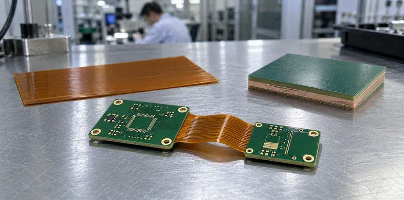
Quick Answer: HDI rigid flex PCB design requires a separate map of the copper layers present in each rigid and flex region. Define every microvia by its layer pair, physical drilling face and fabrication stage, then confirm that filling, planarization and later lamination preserve both the connection and the required surface.
A connection from L4 to L5 can look straightforward in a CAD via definition. On a rigid-flex board, those layers might be the exposed faces of a two-layer flex subassembly before they become internal layers beneath rigid material. The connection therefore has a manufacturing deadline: it must be formed while the intended surface remains accessible.
A regional layer map and a stage-labelled via schedule make that manufacturing deadline visible. The illustrative eight-layer rigid region with a two-layer flex span below shows how layer names, drilling access and surface treatment interact. The fabricator must qualify the actual materials, dimensions and process route.
Table of Contents
- Separate the flex region from the HDI build
- Map global layer names to each physical region
- Give every via an entry face and a build stage
- Turn the connectivity map into a manufacturing sequence
- Protect flex surfaces before fill and planarization
- Choose the drilling side around the finished pad
- Review thickness and geometry one layer pair at a time
- Keep the layer map stable through CAM changes
- Assign inspection to each buried connection family
- Send the regional construction for a quotation
Separate the flex region from the HDI build
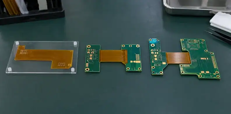
In HDI rigid flex PCB design, the HDI designation describes the interconnect construction, while rigid-flex describes the rigid regions and the continuing flexible layers. The two descriptions answer different design questions, so specify their locations together.
A dense device on a rigid island may need outer-layer microvias even when the connecting flex span uses only two copper layers. Adding those microvias does not automatically add the same build-up layers across the flex span. Conversely, a connection formed within the flex subassembly may later become buried beneath the rigid island. Its finished position does not reveal the stage at which it was made.
Start with component locations and required net transitions. Mark each rigid island, each flex-only region and any region with a different copper population. This establishes where a proposed via family physically exists. A hole whose target layer disappears outside the rigid island cannot simply be moved across that boundary during routing cleanup.
The architecture still has commercial consequences. Our comparison of rigid-flex and flexible PCB costs explains that earlier choice. Once rigid-flex is selected, the immediate task is to prove the individual connections can be built in the intended regions. A global layer count alone cannot provide that proof.
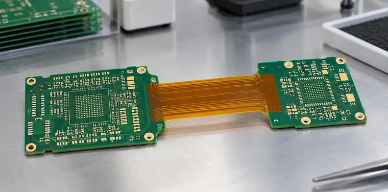
Map global layer names to each physical region
Keep the global copper-layer names, then show which of those layers survive in each physical region. Do not call the flex span “L1–L2” without also identifying its relationship to the full-board layer numbers.
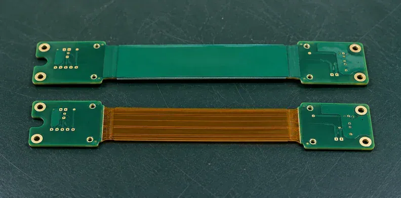
In the example below, the rigid region contains L1 through L8. Only L4 and L5 continue through the flex span. Within that span, L4 and L5 are its outer copper faces; beneath the rigid island, they are internal copper. A description such as “top-side flex microvia” remains ambiguous until the drawing identifies the physical face and global layer.
| Physical region | Copper present | Exposed copper before covering | Consequence for a proposed connection |
|---|---|---|---|
| Rigid island A | L1–L8 | Final outside faces are L1 and L8 | L1–L2 and L8–L7 can be reviewed as outer build-up pairs |
| Flex span | L4 and L5 | L4 and L5 on the flex subassembly | An L4–L5 connection requires access before any later covering blocks it |
| Rigid island above the flex core | L1–L8, including continuing L4/L5 | Surface identity changes as rigid layers are added | A via in the continuing flex core may become buried in the final rigid region |
| A second rigid region with another construction | As explicitly drawn | As defined by its local construction | Reuse a via family only after confirming the same materials and stage access |
The fourth row is a review condition, not an extra region required on every board. Its purpose is to prevent a copied CAD rule from silently crossing into another construction.
General HDI stackup notation describes build-up arrangements. Add this regional map alongside that notation so CAM can relate each drill file to actual copper. Include orientation views or section cuts where the same layer becomes exposed in one region and buried in another.
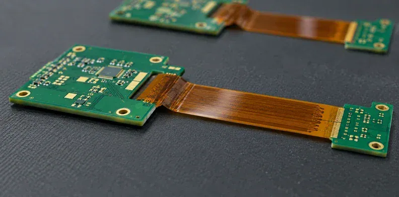
Give every via an entry face and a build stage
A layer pair becomes a manufacturing instruction only when it has a region, drilling direction and accessible build stage. Record those fields before assigning one drill code to all geometrically similar holes.
An L1–L2 microvia and an L4–L5 microvia may both connect adjacent copper layers. They encounter different materials and different surfaces. The first might be formed after an outer build-up dielectric is laminated. The second might belong to the flex core before that core is incorporated into a rigid subassembly. Combining them under one generic “laser via” note hides this distinction.
| Via family | Illustrative global pair | Applicable region | Entry face and timing | Required disposition before the next stage |
|---|---|---|---|---|
| Rigid top build-up | L1 to L2 | Rigid island only | Enter from L1 after its dielectric is added | Plate or fill as approved for the land and subsequent connection |
| Rigid bottom build-up | L8 to L7 | Rigid island only | Enter from L8 after its dielectric is added | Confirm bottom-side land requirements independently |
| Flex-core interconnect | L4 to L5 | Defined locations on the two-layer flex core | Enter from the specified exposed core face | Resolve hole closure and surface needs before covering or embedding |
| Connection inside an intermediate subassembly | Pair shown on the approved subassembly drawing | Region where both layers exist | Form while that subassembly has the required accessible face | Complete its approved treatment before the surface becomes internal |
The table does not imply that every listed family belongs on the example board. It gives each retained family a place in the route.
Use separate family identifiers when the same pair needs different treatments, such as a solder land versus a target for another microvia. The laser-drilled microvia acceptance guide covers cavity and target-pad inspection. The stage record tells the fabricator which cavities those criteria must represent.
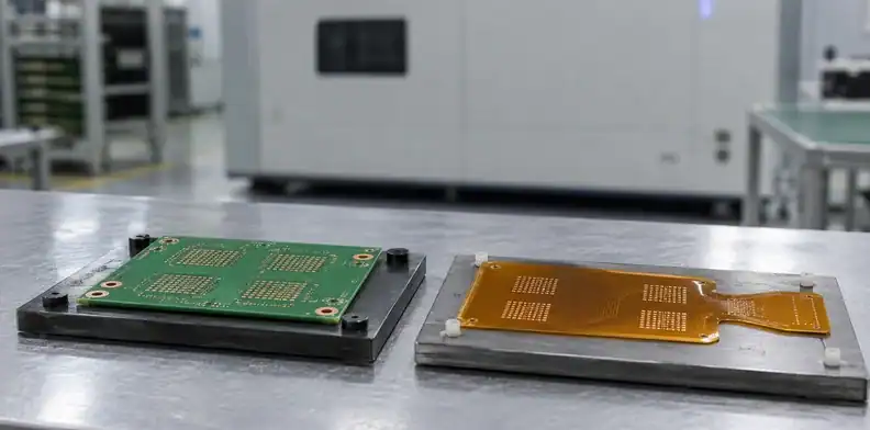
Turn the connectivity map into a manufacturing sequence
Build the sequence around surfaces that will disappear from access. Finish each stage’s required connections and hole treatment before later layers bury them.
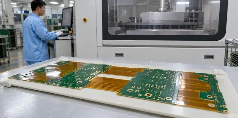
Build the flex subassembly while its faces are accessible
For the illustrative L4/L5 flex core, begin by agreeing on its laminate construction and which face the laser enters. Patterning, hole formation, plating and covering must be ordered by the chosen qualified process. The dependency is that a connection requiring access to L4 or L5 cannot wait until rigid material covers that location.
Distinguish positions within the final rigid island from positions in the exposed flex span. The continuing core may receive different covering or later material in those regions. A single full-panel process note can obscure that regional difference. The fabrication drawing should identify where each operation applies, while the supplier’s route defines how it is executed.
Add rigid layers without losing the earlier connections
Once a surface becomes internal, its condition becomes an input to the next lamination. An open hole, a filled target and a planarized copper surface are different inputs. Decide which one is required before approving the stage that buries it.
| Review stage | Surface or connection available | Decision before proceeding | What a later stage cannot resolve merely by changing a drill file |
|---|---|---|---|
| Flex-core fabrication | L4 and L5 are accessible as core faces | Confirm entry side, local hole treatment and covering sequence | Recover a core face already hidden beneath rigid material |
| Intermediate rigid/flex assembly | Approved internal layers and subassembly faces | Complete required internal connections and inspect their treatment | Correct an inaccessible buried target without changing the construction |
| Outer dielectric build-up | The specified outer laser pairs become accessible | Verify dielectric depth, target identity and any lower filled connection | Substitute another target pad without changing the electrical path |
| Final finishing and profile | Final lands and regional outline | Check that earlier stage dispositions match the finished drawing | Prove a hidden interface was properly formed from appearance alone |
These are dependency checkpoints, not a press recipe. Material flow and bonding need a separate process review; our article on no-flow prepreg lamination control addresses that work. Keep its approved material and process conditions tied to the same construction revision.
Protect flex surfaces before fill and planarization
Review the surface exposed to planarization before choosing the hole treatment. A process that levels a rigid face may damage an unsupported thin flex face in the same subassembly.
Distinguish resin closure from a copper-filled target
PCEA’s Via Viability describes flex constructions in which resin from a later lamination can close buried holes. It also identifies difficulties with conventional fill-and-planarize processing on thin flex material. These observations require a review of the exposed faces; they do not establish one fill method for every flex via.
Specify the purpose of the treatment. Closing a buried opening, providing a flat assembly land and creating a conductive target beneath an upper microvia impose different requirements. Resin closure alone does not provide the same conductive structure as a specified copper-filled target. If another microvia will land on that location, the proposed lower connection and its surface need explicit approval for that role.
Work through an exposed-flex polishing conflict
Consider an illustrative intermediate assembly with a rigid top face and an exposed thin flex bottom face. The proposed route requires filling and planarizing a connection in the rigid region. PCEA discusses the risk of damaging an exposed flex face during such processing, and describes constructions that retain a rigid protective face instead.
Apply that lesson by asking which face contacts the equipment, how the panel is supported and whether the qualified process can protect the exposed flex material. A supplier might propose retaining a rigid cap during this stage, revising the subassembly or relocating the connection. Each option changes a physical feature that the original CAD via definition may not describe.
For this scenario, verification would include the revised section drawing, the supplier’s treatment method and inspection of the relevant surfaces and connections. Those are proposed checks; no test result or yield improvement is assumed. If a cap changes copper participation or dielectric depth, update both the regional map and via schedule before accepting it. The practical lesson is to resolve the vulnerable surface at the intermediate stage, while there is still a construction choice to make.
Choose the drilling side around the finished pad
Choose the drilling face with the final pad function in view. The laser entry surface and the assembly land are separate fields, even on a two-layer flex construction.
For some two-layer flex constructions, the PCEA discussion shows drilling from the side opposite an SMT pad to preserve the pad’s original foil surface. That observation is a useful design question, not permission to omit hole treatment in every solder land. The finished opening, plating, closure and assembly requirements still need review.
Take the illustrative L4/L5 core. If the component land is on L4, identify whether entry from L5 is physically available at the intended stage. Then confirm what remains at L4 after the hole and plating processes. “Via in pad” alone does not say whether the assembler receives an opening, a capped surface or another agreed condition.
Also distinguish an assembly pad from a pad that receives a later microvia. A route suitable for one function may not satisfy the other. Our discussion of stacked and staggered microvias covers the connection choice. Here, carry the chosen arrangement into the stage schedule so every upper via has an approved lower target at the time it is formed.
When the drilling side changes, revisit access, registration references and surface treatment together. A flipped entry arrow may require more than a new drill instruction.

Review thickness and geometry one layer pair at a time
Use the local construction for each pair’s depth and geometry review. Finished board thickness does not describe the dielectric traversed by a particular microvia.
The flex-core pair and the outer rigid build-up pair need separate material records. Qnity’s current Pyralux AP product information identifies an adhesiveless all-polyimide laminate and lists constructions with different copper and dielectric thicknesses. “Polyimide core” therefore leaves the local copper and dielectric unspecified. This material example does not confirm QueenEMS stock or approval for a proposed route.
| Field to confirm | Why it belongs to the individual pair | Evidence to use |
|---|---|---|
| Dielectric identity and local thickness | Determines the material and depth encountered by that hole | Material designation and approved local section |
| Copper on the entry and target layers | Affects the drilled surface, target and finished land | Starting copper construction and finished copper requirements |
| Hole dimensions and measurement convention | A nominal CAD diameter may differ from the reported cavity dimension | Supplier drawing and acceptance convention |
| Capture and target land geometry | Must accommodate the actual hole and local registration conditions | CAM review linked to that via-family identifier |
| Fill, cap and surface condition | Determines suitability for the next layer or assembly land | Approved treatment note and representative inspection |
The microvia aspect-ratio calculation guide explains the measurement terms. Apply them to the relevant local pair rather than borrowing a value from another region. Ask the fabricator to state the supported geometry for the proposed material and route; a dimensional limit from a different construction is insufficient evidence.
Keep the layer map stable through CAM changes
Approve CAM changes by comparing physical layer identity and connection path, not just the revised total layer count. A construction revision can preserve the netlist while changing the route used to build it.
Check physical layers after a supplier adds a cap
A proposed cap may add material or copper, change an intermediate outer face, or require a different layer-number convention. Ask for a before-and-after cross-section that identifies the continuing flex layers in both versions. Decide whether the cap remains in the delivered board or is a process feature, and record that distinction in the approved drawing.
Keep a mapping from CAD layer names to the revised physical layers. If the supplier renumbers the construction, an unchanged label such as L4–L5 may now refer to another physical pair. Check drill spans, pad locations and regional copper presence against the mapping. The same check must include impedance-controlled layers when their local dielectric environment changes.
Treat a moved via as a changed connection path
Moving a via to avoid an exposed flex face can alter the local construction even if its net remains unchanged. Confirm that both target layers exist at the new location and that the approved entry surface is available at the scheduled stage. A relocation into the rigid island may also change the connection’s depth or covering.
Our HDI lamination registration budget article explains alignment allocation through successive stages. Tie that review to the revised pair and region. Layout engineering should approve electrical and land changes; fabrication engineering should confirm the route; quality should accept the corresponding evidence plan. Close the CAM question with the revised files and drawing, rather than leaving the original drill note beside an incompatible supplier stackup.
Assign inspection to each buried connection family
Map inspection evidence to the connection families created at each stage. One attractive cross-section does not establish that every regional interconnect has the same construction or performance.
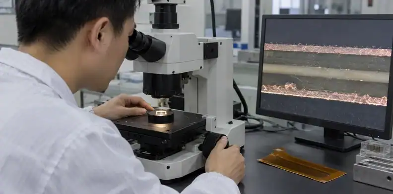
An outer rigid microvia, a flex-core connection and a filled lower target may encounter different materials and processing histories. Coupon placement and construction should represent the features being accepted. Where one coupon covers several families, ask the supplier to identify exactly which layer pairs and treatments it represents.
| Connection family or feature | Evidence question | Limitation to address |
|---|---|---|
| Flex-core connection before burial | Does the inspected sample use the same local laminate and hole treatment? | A rigid-only coupon may not represent this core |
| Outer rigid microvia | Does the section confirm the intended target and cavity construction? | It says little about a separate buried family |
| Lower filled connection beneath another microvia | Is the target interface represented in the inspection and electrical test structure? | Surface flatness alone does not establish interface performance |
| Revised protective-cap construction | Does inspection match the approved cap and layer map? | A result from the original route may no longer be representative |
| Completed interconnect chain | What performance test and acceptance limits apply to this construction? | Initial continuity does not measure every latent failure mechanism |
IPC’s microvia reliability warning explains that conventional microsection inspection can miss weak interfaces that fail later under thermal exposure. It supports adding appropriate performance evidence; it does not supply a universal qualification recipe for this board.
Use the microvia thermal-cycling qualification guide for the test-method discussion. In the regional schedule, record which families the agreed test covers, the construction revision and the acceptance report to be delivered.
Send the regional construction for a quotation
Request a quotation against one consistent regional map and via-family schedule. Leave proposed supplier deviations visible until engineering approves their effect on the connection and build order.
Make the first build answer a construction question
For a new combination of flex-core microvias and rigid build-up layers, state the unresolved question precisely. It might concern the exposed flex surface during planarization, an upper microvia’s lower target, or the availability of a drilling face before burial. Give the supplier the relevant section and family identifier rather than asking whether it can manufacture “HDI rigid-flex” in general.
Define what evidence will close that question during the first build: a representative section, a verified pad condition, the agreed electrical performance result or another construction-specific acceptance item. Assign the engineering approver. A successful sample proves only the agreed scope and construction; retain its revision so later material or route changes receive a deliberate review.
Compare quotations against the same layer-pair set
Send the regional copper map, complete stackup, via-family table, drill definitions, assembly-land requirements and material identifications together. Include the intended finish, quality requirements, order quantity and required delivery date. Ask each supplier to list construction changes, added stages, exclusions and qualification work in its response.
A quotation with fewer stages may rely on a changed via location or surface treatment. Compare that change with the electrical design and acceptance plan before treating the prices as equivalent. Keep assumptions about cap layers, buried-hole closure and upper targets in the quotation record; they affect what will arrive for assembly.
To request a construction review from QueenEMS, send these files through our contact page and identify the layer pairs or intermediate surfaces that remain unresolved. The resulting review should establish an agreed route and evidence scope before the order is released.

Written by the QueenEMS Engineering Team
Upload your files today · Free DFM check before production · Ship worldwide
Get your PCB prototypes in as fast as 24 hours. We handle FR4, Rogers, and hybrid boards up to 40 layers in volume production, with advanced builds subject to engineering review — free prototypes for 2–4 layer FR-4 boards, no minimum order.
Just upload your Gerber + BOM — we source every part, assemble, and inspect (AOI + X‑Ray) so you don't have to chase suppliers. Boards ship in as fast as 24 hours.