
Warpage grows across the long diagonal
Asymmetric copper, unbalanced stack-ups and residual lamination stress can push corners outside flatness limits.
Control: copper-balance review, symmetric construction and panel-level flatness measurement.
As a large format PCB manufacturer, QueenEMS supports custom oversized PCB fabrication for industrial, power, LED, communication and test-equipment projects. Qualified 1–2 layer boards can reach 2000 × 600 mm, while qualified 4–10 layer boards can reach 1400 × 540 mm. All maximum-size projects require engineering confirmation before quotation.
Know your outline and layer count? Get a buildable answer before committing to tooling or material.
Check My Large PCB FeasibilityA large format PCB is a board whose finished outline exceeds the comfortable process window of standard PCB equipment. The values below describe maximum finished-board envelopes, not raw laminate or production-panel dimensions. Actual feasibility changes with layer count, lamination route, material, copper weight, finish and testing method.
| Layer count | Maximum finished board size | Qualification status |
|---|---|---|
| 1–2 layers | 2000 × 600 mm | Engineering confirmation |
| 4–10 layers | 1400 × 540 mm | Engineering confirmation |
| 12+ layers | Confirmed by stack-up and process | Consultation required |
Important: these values describe maximum finished-board envelopes, not production-panel or SMT assembly limits. Material, thickness, copper weight, surface finish, via structure, test method and quantity may reduce the buildable size. Written engineering confirmation is required before quotation or order release.
Send your exact outline, layer count and finish to confirm which row applies to your design.
Confirm My Maximum Board SizeThe outline may fit a machine while the complete process route does not. These six failure modes are checked before a custom large PCB is released.
Asymmetric copper, unbalanced stack-ups and residual lamination stress can push corners outside flatness limits.
Control: copper-balance review, symmetric construction and panel-level flatness measurement.
Material movement accumulates across long dimensions and reduces annular-ring or impedance margin.
Control: material-specific compensation, datum planning and inner-layer inspection.
Dense and open copper regions can plate differently across an oversized panel, affecting hole copper and trace geometry.
Control: current-density planning, thieving strategy and lot-specific verification.
Coating, exposure and handling become harder to keep uniform when the panel exceeds standard working dimensions.
Control: process-window confirmation, registration targets and final opening inspection.
A manufacturable circuit can still fail when the profile, V-score direction or tooling rails exceed machine travel.
Control: mechanical-drawing review, datum confirmation and route-specific tooling.
Large boards need more support area and can be damaged by point loads, edge impacts or uncontrolled stacking.
Control: flat support, interleaving, edge protection and carton-level handling instructions.
Let engineering identify the limiting process before material is purchased.
Request a Large PCB Risk ReviewThe correct manufacturing route depends on why the board is large—not only on the final length and width.
Oversized rigid boards for controllers, equipment interfaces, backplanes and distributed power or signal functions.
Review focus: Tg, thickness, copper balance, panel support and finish.
Long, narrow boards used where one continuous circuit avoids connectors, cable assemblies or multiple joined boards.
Review focus: long-axis routing, V-score direction, handling and packing.
Multilayer oversized PCBs whose permitted outline reduces as lamination complexity and registration demand increase.
Review focus: stack-up symmetry, material movement and maximum panel size.
Power-distribution designs requiring more copper, greater heat capacity or mechanically robust conductors.
Review focus: copper weight, line/space, plating, etch and thermal balance.
Square, circular, spiral or custom planar coils using FR-4, RF laminate or flexible base materials.
Review focus: copper uniformity, resistance targets, spacing and test method.
RF, antenna and low-loss structures where sheet availability and dielectric consistency constrain the practical size.
Review focus: laminate model, grain direction, impedance coupons and loss targets.
Tell us what makes the board large so we can select the right process route.
Discuss My Large PCB TypeLarge-board architecture can reduce connectors, cable assemblies and board-to-board interfaces—but only when mechanical support, serviceability and yield are considered together.
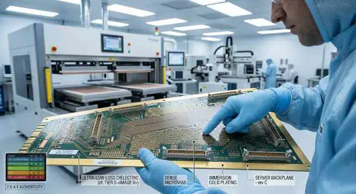
Connector-dense control and data distribution boards for racks, test systems and industrial computing.
Common need: registration, connector alignment and flatness.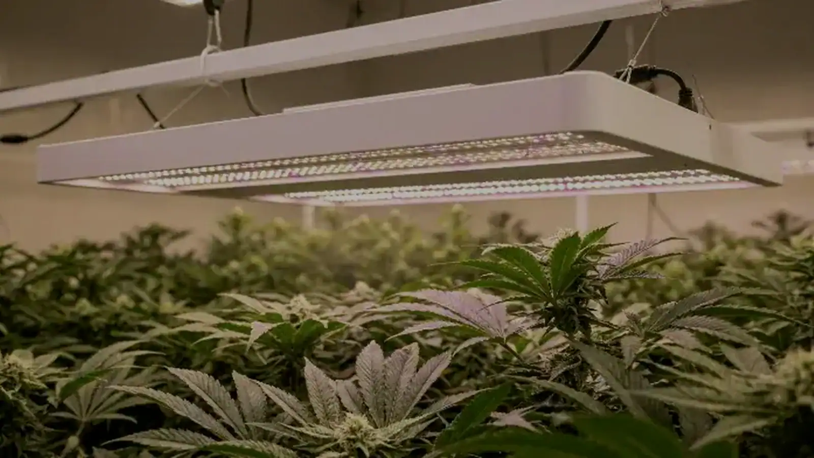
Long or wide lighting boards that simplify series connections and maintain consistent emitter spacing.
Common need: extra-long outline, thermal balance and panelization.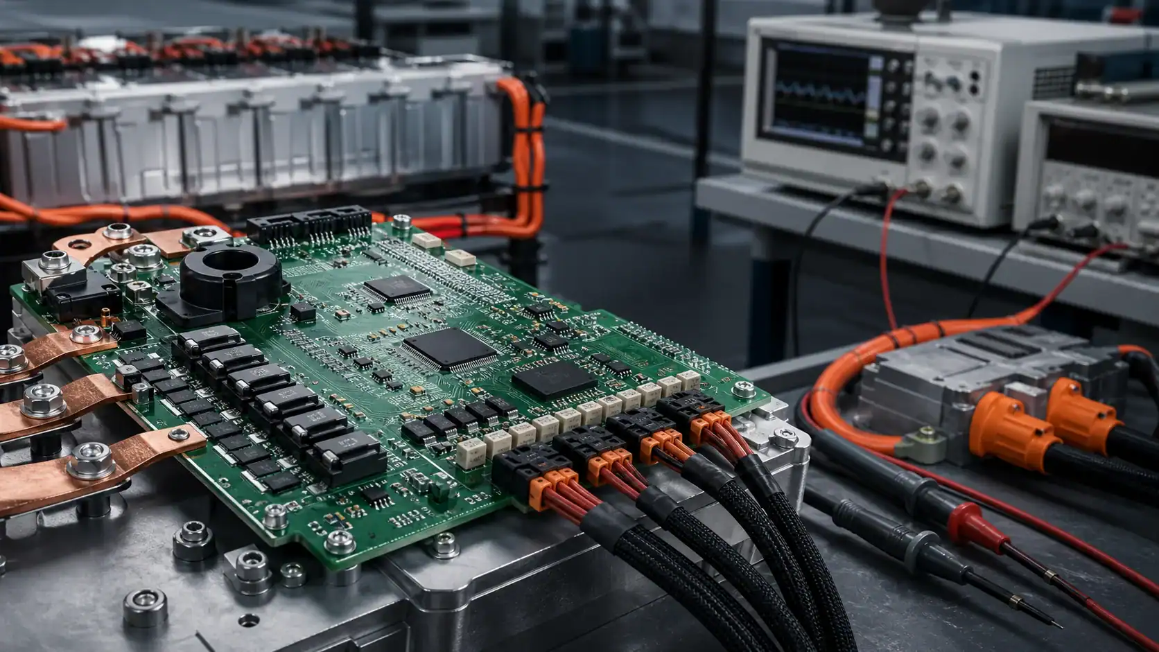
Power distribution, battery, inverter and charging designs requiring more copper and board area.
Common need: heavy copper, spacing and transport support.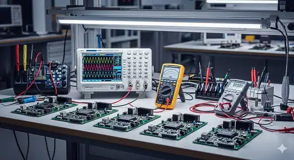
Fixture interfaces, channel-dense test boards and large signal-routing structures.
Common need: datum accuracy, impedance and replaceable wear areas.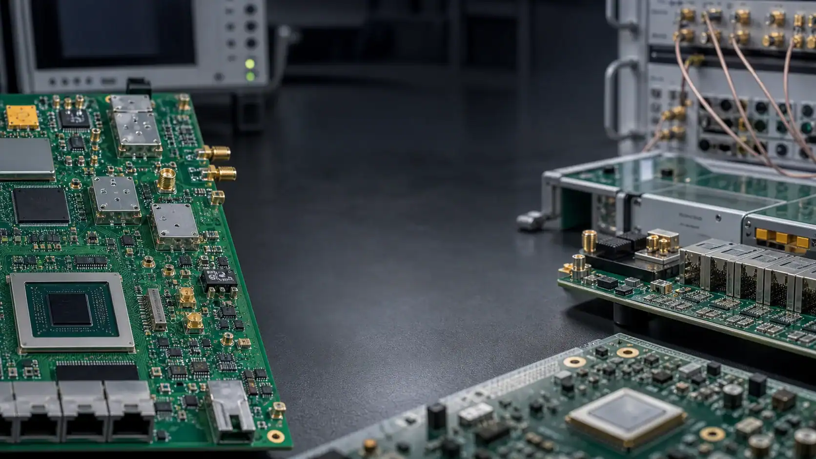
RF, antenna, base-station and network infrastructure with long signal paths or distributed connectors.
Common need: low-loss material, impedance and dimensional stability.
Machine-control, sensor-distribution and motion systems where one board can simplify internal wiring.
Common need: vibration, connector placement and service access.Share the end use so the size review includes mechanical, electrical and shipping conditions.
Review My ApplicationAn oversized outline does not automatically inherit the full material and process list of a standard board. Sheet size, press format, copper weight and finish line must be qualified together.
KB and Shengyi FR-4 options for industrial and general electronic products, subject to the selected Tg and sheet format.
Best starting point for maximum-size qualification.Higher-temperature and compliance-focused systems for thermal cycling, industrial or regulated applications.
Confirm exact laminate model before fixing the outline.Low-loss and hybrid material systems for antennas, telecom and signal-sensitive large boards.
Sheet availability and hybrid press route require review.Published standard ranges cover common copper weights; heavier copper changes minimum line/space, etching and plating requirements.
Maximum outline may reduce as copper weight rises.ENIG, HASL, OSP, hard gold, ENEPIG and selective-gold routes can be evaluated against the board size and end use.
Finish-line envelope must match the production panel.Impedance, controlled-depth features, resin plugging, blind/buried vias and HDI are available only within qualified combinations.
Advanced processes do not automatically support the maximum published board length.Compatibility rule: qualify the complete build—size, layers, thickness, copper, laminate, surface finish, via structure and testing—not one parameter at a time. For example, published resin-plugging capability lists standard single-board length up to 650 mm, with longer designs requiring evaluation.
Send the laminate model and copper requirement before the mechanical outline is frozen.
Check Material & Size CompatibilityLarge PCB warpage control begins in the design. A feasible outline can still have poor yield if copper, stack-up, tooling and handling decisions are left until CAM.
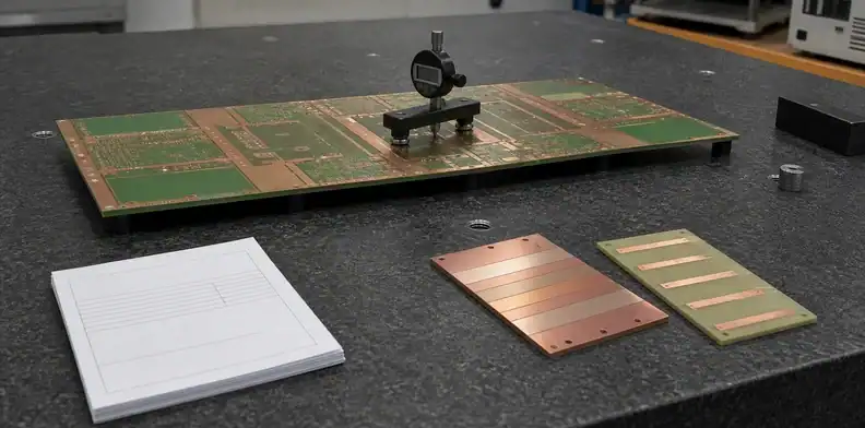
Avoid large density differences across the board and between opposing layers.
Keep core, prepreg and copper distribution mechanically balanced around the center.
Define stable handling and datum areas that survive the complete process route.
The V-score axis and residual thickness must fit the published equipment envelope.
Identify which holes, edges and connector locations control system-level fit.
Plan impedance, microsection or plating coupons without exceeding the panel window.
Keep critical features away from routing, depaneling and packaging contact zones.
Large bare-board capability does not guarantee the same SMT conveyor or fixture size.
A short DFM review now can prevent a full-panel scrap decision later.
Send My Gerber for Large PCB DFMThe standard PCB sequence remains familiar, but each step needs equipment travel, material support and uniformity controls suitable for the larger working area.
Verify laminate model, sheet condition, copper and available cutting orientation.
Large-format control: sheet size and directional planning.Transfer and form circuit geometry across a larger exposure area.
Large-format control: registration and exposure uniformity.Bond multilayer constructions while managing thermal stress and material movement.
Large-format control: balanced stack-up and press envelope.Create through-holes and mechanical features using a qualified datum strategy.
Large-format control: machine travel and positional accuracy.Build hole-wall and surface copper across dense and open circuit areas.
Large-format control: current-density and thickness uniformity.Coat, expose, cure and finish the production panel within line limits.
Large-format control: coating support and finish compatibility.Create the final outline and controlled breakaway features.
Large-format control: long-axis direction, rails and datum.Verify continuity and isolation, then protect the finished board for transit.
Large-format control: test-field size and full-area support.Ask which process—not just which machine—sets the limit for your board.
Review My Manufacturing RouteA credible oversized PCB manufacturer should explain what is measured, when it is measured and what evidence can be linked to the lot.
Confirm laminate identity, copper foil and relevant incoming condition.
Possible evidence: CoC, material lot and incoming record.Detect opens, shorts and geometry defects before lamination locks them inside.
Possible evidence: AOI disposition or inspection record.Verify layer-to-layer and drill-to-pattern margin on qualified locations.
Possible evidence: dimensional or registration data.Check hole-wall copper, interface condition and relevant stack-up features.
Possible evidence: cross-section images and readings.Verify the outline and critical mechanical datums identified on the drawing.
Possible evidence: FAI or dimension report.Measure bow and twist using the agreed support and acceptance method.
Possible evidence: lot flatness record.Confirm continuity and isolation within the available large test field.
Possible evidence: electrical test result or log.Check full-area support, separation, edge protection and shipment labels.
Possible evidence: packaging photos and release record.Evidence is project-specific. Define the documents you require at RFQ stage. Not every report is automatically included with every order, and acceptance criteria should be agreed before production.
Tell us which reports your quality team needs for first-article or lot release.
Build My Quality Evidence PlanThe images below show the types of manufacturing and inspection evidence relevant to a size-sensitive project. Your own order should be supported by lot-specific records agreed during quotation.
Use a clear dimensional reference, approved stack-up and material identity—not an unlabeled board photograph.
Verify: size, layers, material, thicknessRecord the measurement method, support points, result and applicable acceptance limit.
Verify: bow, twist, method, limit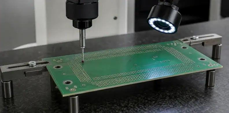
Measure the holes, edges and connector features that control mechanical integration.
Verify: drawing datum and FAI points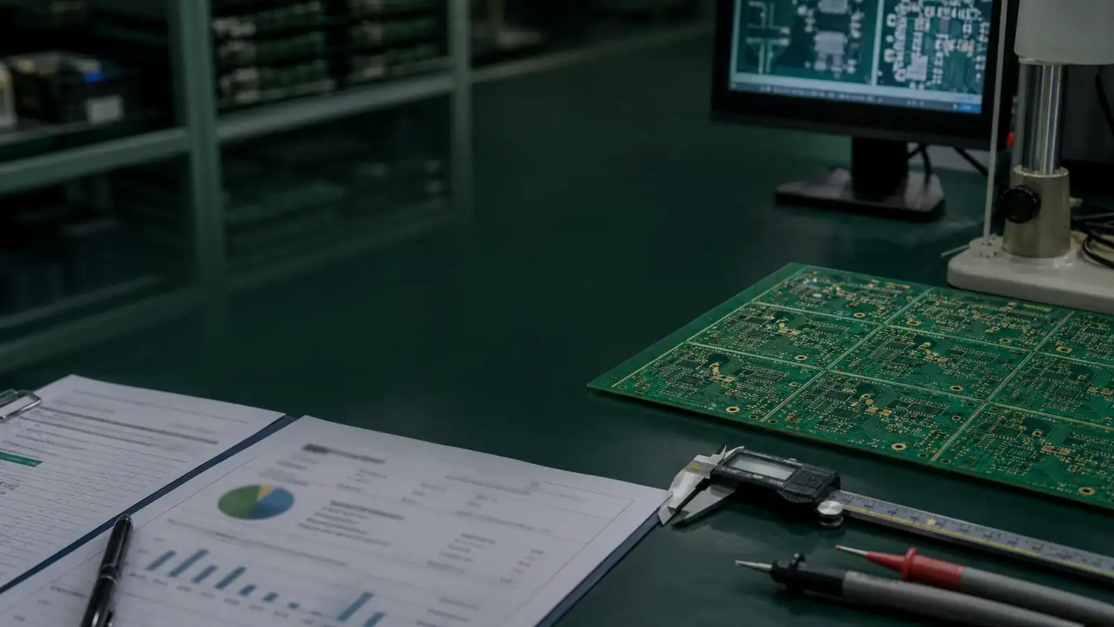
Link test, dimension and outgoing records to the actual production lot and revision.
Verify: lot identity, revision, release statusDefine the proof package for your first build before the purchase order is released.
Request First-Article EvidenceThere is no responsible fixed price per board without the production-panel plan. Large PCB cost is driven by usable area, process fit, yield risk and the support needed through testing and transit.
The board outline may consume most of a production sheet while leaving unusable strips or requiring special cutting orientation.
Cost effect: material area and yield per panel.More layers add imaging, inspection, lamination and registration work while reducing the available size window.
Cost effect: process steps and qualification risk.Non-standard laminate models, high-Tg, RF or halogen-free sheets may have different usable dimensions and lead times.
Cost effect: sheet price, MOQ and procurement time.Heavy copper and special finishes add process constraints and may change line/space or production-panel feasibility.
Cost effect: chemistry, cycle time and scrap exposure.Large test fields, dedicated fixtures and project-specific reports should be defined in the RFQ.
Cost effect: fixture, inspection and reporting scope.Rigid support, oversize cartons, dimensional-weight freight and destination handling affect the delivered price.
Cost effect: packaging design and volumetric freight.Confirm the full process route, not only the outline.
Secure the qualified sheet, CAM data and test route.
Run the approved process and hold points.
Protect the full board area through the selected route.
Exact prototype and production lead times are issued after engineering confirms the layer-dependent size, material availability and inspection scope.
Get a quote based on the real production panel, quality plan and shipping method.
Price My Large PCB ProjectA complete RFQ lets engineering answer the real question—whether the full construction can run at the requested size—without repeated clarification loops.
Provide Gerber or ODB++, drill data, mechanical drawing and the target stack-up.
Check size, layers, material, copper, finish, testing and packing as one route.
Resolve manufacturability questions and record any approved changes before release.
Receive the confirmed production route, commercial quote and expected lead time.
Upload these inputs once and receive a more reliable feasibility answer and quote.
Prepare My Large PCB RFQThe value is not a generic “large board” promise. It is a controlled path from customer files to a qualified manufacturing route, documented changes and a protected shipment.
Size, layers and special processes are reviewed before a commercial promise is made.
You receive: questions, limitations and the qualified route.Material or process alternatives are presented for approval instead of being changed without notice.
You receive: an auditable decision trail.Inspection reports and first-article requirements are agreed before production rather than requested after shipment.
You receive: the evidence your release process expects.Approved material, stack-up, DFM decisions and acceptance criteria can carry into repeat orders.
You receive: a clearer repeat-build baseline.Engineering, commercial questions, quality requirements and delivery expectations remain connected.
You receive: fewer handoff gaps and clarification loops.Support, interleaving, edge protection and freight method are treated as part of product delivery.
You receive: packaging matched to board size and route.Work with one team from feasibility questions through first-article release and shipment.
Talk to a Large PCB EngineerPanel size limits for every board type are listed in our PCB fabrication capabilities.
Direct answers to the questions engineers and buyers ask before contacting a large format PCB manufacturer.
A large format PCB exceeds the comfortable finished-board or production-panel window of standard PCB equipment. In sourcing practice, the important threshold is not a universal number; it is the point where your outline, layers and process require dedicated equipment or engineering qualification.
The maximum finished-board envelope for qualified 1–2 layer builds is 2000 × 600 mm. Final feasibility still depends on material, thickness, copper, surface finish, drawing requirements and the complete process route, so written engineering confirmation is required.
Multilayer boards require imaging, inner-layer inspection, lamination, registration and additional handling. Press format, material movement and alignment margin therefore reduce the qualified outline as layer count and stack-up complexity increase.
The maximum finished-board envelope for qualified 4–10 layer builds is 1400 × 540 mm. This does not apply automatically to every stack-up or special process. Boards with 12 or more layers require project-specific consultation.
Large PCB warpage control combines symmetric stack-up planning, copper-density balance, appropriate material selection, controlled lamination, stable handling and panel-level measurement using an agreed acceptance method.
Yes, qualified large heavy copper PCB combinations are possible. Increasing copper weight changes minimum line/space, plating, etching, thermal balance and sometimes the maximum manufacturable size, so the full design must be reviewed.
Rogers, other high-frequency laminates and hybrid constructions can be evaluated. The exact laminate model, sheet availability, grain direction, press route, impedance target and coupon area determine the usable production size.
Flying-probe or fixture-based electrical testing is selected according to size, pad geometry, quantity and available test field. The test route should be confirmed during quotation rather than assumed from standard-board capability.
PCB assembly can be reviewed separately, but bare-board maximum size must not be treated as an SMT assembly limit. Share component placement, board thickness, weight, panel support and required SMT/THT processes so conveyor, stencil, fixture and reflow compatibility can be confirmed.
Provide Gerber or ODB++, NC drill data, mechanical drawing, layer count, stack-up, laminate, finished thickness, copper weight, finish, impedance or special process requirements, quantities, acceptance documents and delivery target.
Have a size or process combination not answered here? Send it for a written engineering response.
Ask My Large PCB QuestionUpload the project package and receive a feasibility review covering the finished outline, layer-dependent size, material route, major DFM risks, inspection scope and quotation inputs.