
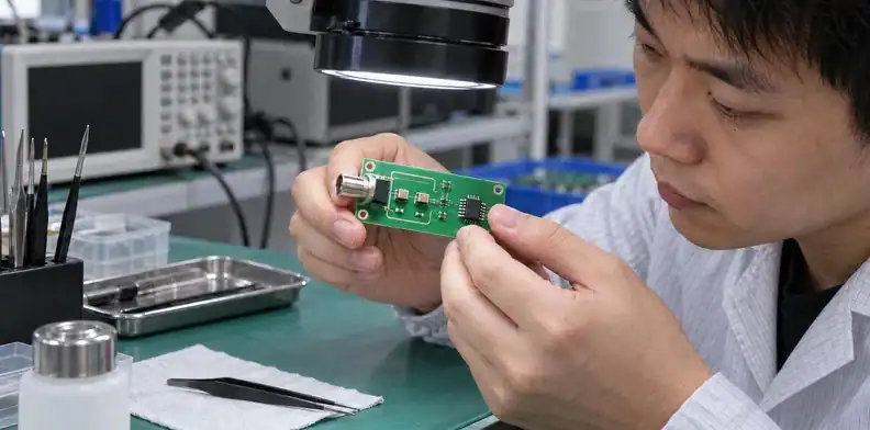
Quick Answer: A PCB guard ring for a high-impedance input is a conductor held near that input’s voltage by a suitable low-impedance source. It intercepts leakage paths around the sensitive node. Select its drive from the actual circuit, extend it along the vulnerable input connection, and specify copper, exposed surfaces and clean handling separately. A grounded perimeter used for EMI has a different purpose.
“Connect the ring to ground” can be correct for one circuit and wrong for another. A photodiode amplifier biased above ground and a unity-gain sensor buffer do not necessarily need the same guard potential.
Begin the leakage-control review with the error budget and schematic. They determine the guard’s voltage and the current paths it must intercept, then provide requirements for layout, manufacturing and test.
Table of Contents
- Decide whether the problem is input leakage
- Estimate the leakage current the circuit can tolerate
- Choose a guard voltage from the actual circuit
- Enclose the complete sensitive path
- Release separate copper, mask and paste instructions
- Control laminate and protective-coating changes
- Protect the guarded area through assembly
- Continue the guard through connectors and cables
- Qualify leakage in the complete measurement setup
- Send a guard-specific fabrication and assembly package
Decide whether the problem is input leakage
Use a PCB guard ring for leakage control when unwanted current entering a high-impedance node threatens the measurement error budget. Identify the vulnerable net, its operating voltage and the surrounding conductors that could supply that current.
The word “guard” also appears in discussions of grounded traces between digital signals and perimeter copper for EMI. Those structures may address electromagnetic coupling, but they do not automatically provide the voltage relationship needed for a leakage guard. Keep their purpose and net assignment distinct in the schematic and layout notes.
Analog Devices’ precision-layout article describes both leakage and thermocouple effects. A drifting low-voltage reading can arise from thermal gradients, while a high-resistance sensor can be sensitive to tiny unwanted input currents. Guarding the input does not remove every source of offset or noise.
List the error contributors before changing the board: amplifier bias current, sensor leakage, protection-device leakage, feedback-component behavior, board leakage and fixture effects. The purpose is to reserve an allowance for each contributor and determine which the proposed guard can influence.
For a pH electrode interface, for example, inspect the connection from the high-resistance sensor to the amplifier input. For a photodiode current measurement, inspect the summing node and the feedback component. Both can need guarding, but their operating references and measurement sequences can differ substantially. A ring drawn around the whole board would leave those local decisions unanswered.

Estimate the leakage current the circuit can tolerate
Translate the permitted measurement error into an input-current allowance before drawing the guard. This gives the layout review a scale for evaluating contamination and voltage mismatch.
Convert input leakage to output error
For a DC transimpedance stage, an unwanted current at the summing node contributes an output error whose magnitude is approximately that current multiplied by the feedback resistance, within the circuit’s valid operating conditions. With an illustrative 100 MΩ feedback resistor, 5 pA corresponds to 0.5 mV. If the assigned board-leakage allowance were 0.1 mV, the corresponding current allowance would be 1 pA.
These values are assumed for the example. The final budget must account for the actual feedback resistor, amplifier behavior, intended bandwidth and other current contributions. The input protection circuit may already consume much of that allowance before PCB leakage is considered.
Read a guard-mismatch calculation
Microchip AN1258 models parasitic leakage paths with resistances and explains how a near-equal guard potential reduces the voltage across a remaining path.
Consider a deliberately simplified example: 5 V across an assumed 1 TΩ path gives 5 pA using I = ΔV/R. If the same path instead experiences a 10 mV guard-to-input mismatch, the calculated current is 10 fA. With the illustrative 100 MΩ feedback resistance, that contribution becomes 1 µV.
The parasitic resistance is assumed, environmental conditions can change it, and other leakage paths remain. Include guard-to-input voltage mismatch in the prototype test. Measure whether the actual guard follows the input adequately and whether the assembled circuit meets its total error allowance.

Choose a guard voltage from the actual circuit
Drive the guard from a suitable low-impedance source close to the protected node potential. The correct source follows the amplifier configuration and input reference.
| Circuit situation | Voltage relationship to review | Mistake to avoid |
|---|---|---|
| Unity-gain sensor buffer | Output can track the sensitive input within its operating errors | Assuming tracking outside the valid input or output range |
| Noninverting amplifier with gain | Select a supported node or guard driver near the input voltage | Driving the guard from an output at a different voltage |
| Ground-referenced transimpedance stage | Summing node remains near its defined ground reference | Treating every TIA as ground referenced |
| Biased transimpedance stage | Summing node remains near the applied reference voltage | Replacing that reference with board ground |
| Dedicated guard-buffer device | Follow the device’s guard-output configuration and loading limits | Assigning the guard output as an ordinary signal or ground net |
For a biased photodiode circuit, write the summing-node reference explicitly beside the guard-net name. “Virtual ground” describes the feedback-maintained relationship to the reference input; that reference may be above board ground.
Document what happens during startup, input overrange and any mode in which the amplifier leaves its normal operating range. A guard selected only from the nominal DC condition may stop tracking during those events. The circuit designer should decide which conditions need valid measurement and which require recovery time.
Use distinct net names for guard and signal return. A general ground-plane review can clarify the board reference, but the guard net must retain its circuit-specific assignment through CAD, CAM and test.
Enclose the complete sensitive path
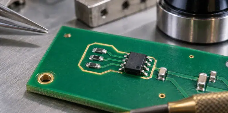
Guard the connected high-impedance path, including the input pin, sensor connection and relevant component lands. Trace the net in the layout instead of using the IC outline as the boundary.
| Vulnerable feature | Layout review | Possible omitted path |
|---|---|---|
| Amplifier input pin | Nearby pins, exposed lands and guard access | Leakage from an adjacent powered pad |
| Sensor trace | Surrounding conductors along its length | An unguarded connection before the ring |
| Feedback component | Identify the high-impedance end | Ring encloses the package but misses the sensitive land |
| Through-hole connection | Inspect both board surfaces and the pad stack | Exposed bottom-side input land |
| Internal-layer neighborhood | Review nearby voltages and dielectric paths | Bulk path beneath otherwise guarded surface copper |
For a photodiode amplifier, distinguish the summing-node end of the feedback resistor from its output end. The guard’s role is to intercept leakage into the sensitive connection, so package placement and land spacing must allow the guard to pass where required.
Keep the sensitive net short where the circuit permits. Adding a test pad or routing detour creates another exposed feature that needs analysis. A convenient probe point can also make the measurement more susceptible to contamination and fixture loading.
Review both surfaces when the connection crosses the board. Surface guarding does not eliminate all leakage through the dielectric. Where a device reference design uses guard planes or vias, preserve their net identity and review the complete stackup. Copying the visible top-layer ring alone leaves the internal structure unspecified.
Release separate copper, mask and paste instructions
Specify the guard copper and its surface exposure separately from the solder-paste pattern. These are separate manufacturing decisions even when they describe the same location.
Expose only the intended guard surface
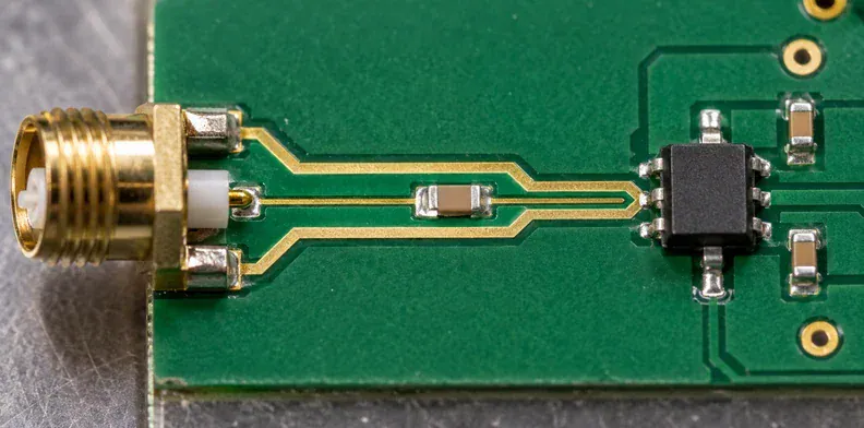
The cited precision-layout guidance uses an exposed guard to intercept surface leakage. Translate that requirement into a defined region in the solder-mask data, including the intended relationship to nearby input lands. The mask-opening requirements page explains the generic registration and copper-exposure interface; the guard drawing supplies the local purpose.
An expansion or automatic mask edit can expose additional copper beside the guard. Review that change against the actual high-impedance geometry before approval. Keep the exposed region limited to the approved design, with its surface finish identified in the fabrication specification.
Keep paste openings tied to actual solder joints
A Fedevel discussion about guard-ring creation records a user’s confusion between mask removal, paste and the appearance of finished copper. The manufacturing lesson is to inspect each exported layer independently.
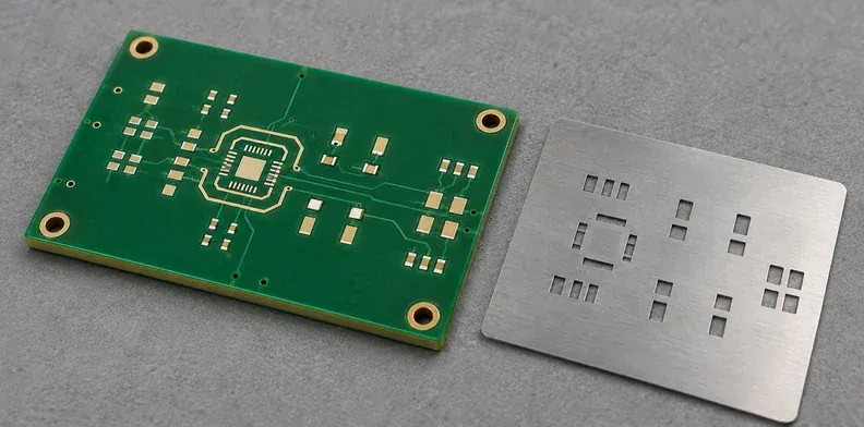
An exposed trace does not by itself request a solder-paste deposit. Show the paste apertures for component joints and check that a copper or mask edit has not created unintended deposits along the guard. Also distinguish the delivered bare-board finish from solder later added during assembly.
Before production, compare the CAM output with the approved guard-region drawing. Resolve any question about net assignment, exposure or deposit geometry in a revision-controlled response. Use the CAM question closeout process to retain that approval with the board files.
Control laminate and protective-coating changes
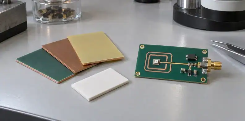
Qualify material and coating choices against leakage under the intended environmental conditions. A laminate’s nominal thickness and Tg do not fully describe its suitability for a sensitive measurement.
| Proposed change | Evidence needed | Approval question |
|---|---|---|
| Laminate substitution | Exact material, stackup and relevant electrical/environmental data | Does the measurement still meet its leakage budget? |
| Mask product or process change | Local exposure map and comparison plan | Has the sensitive surface relationship changed? |
| Conformal coating addition | Material, coverage boundary and qualified process | What happens to leakage and settling after coating? |
| Coating repair | Repair material and local process history | Which measurement must be repeated? |
| Stackup rearrangement | Nearby conductor potentials and dielectric geometry | Has a bulk leakage path changed? |
The ADI UG865 evaluation-board guide documents a particular hybrid construction using RO4350B layers and an FR-4 core. That is a device-specific example, not evidence that every guard requires the same laminate.
Treat an equivalent-material proposal through controlled material substitution approval. Identify the electrical property and environmental test that matter for this circuit.
Coating also needs a local decision. It can protect a surface while introducing its own dielectric and leakage behavior. Define any guarded-area exclusion in the drawing and evaluate the actual coverage. The broader conformal-coating selection guide addresses process choices; the measurement qualification determines whether a particular choice works here.
Protect the guarded area through assembly
Make the guarded region a controlled handling and process area from assembly through final test. Its copper can be correct while fingerprints, residues or a repair change the measurement.
Mark the boundary in assembly documentation and show acceptable handling locations outside it. A fixture should support the board without contacting sensitive surfaces unnecessarily. Avoid adding removable labels, temporary adhesive or informal bench markings inside the region.
Specify the qualified cleaning and drying process with the manufacturing team. A procedure from an evaluation-board manual belongs to that board and its materials; it should not become a universal solvent or baking instruction. Define the compatible process and the electrical check that verifies the result for the proposed assembly.
Review the limits of ionic-cleanliness test reports when selecting lot evidence. A bulk extraction result can be useful process information, while the actual input-leakage requirement still needs a circuit-appropriate check.
Repair deserves an explicit restart point. Record the touched components and local process, repeat the approved cleaning where required, and rerun the affected measurement after the documented settling period. Keep the result with the repair history.
For a sensor-input board stored before final assembly, specify handling and storage conditions that support the intended test. If the board is tested dry and then handled or coated, that earlier result describes the earlier state. Quality should identify the final accepted condition and preserve it through packing and shipment.

Continue the guard through connectors and cables
Assign each connector conductor according to the measurement circuit and instrument configuration. A cable shield can serve as guard, signal return or an electrostatic enclosure, depending on the connection.
| Connection feature | Function to name | Item to verify |
|---|---|---|
| Triax center conductor | Sensitive input | Complete high-impedance path and termination |
| Triax inner shield | Guard where the circuit specifies it | Selected driver and allowed loading |
| Triax outer shield | Defined return or enclosure connection | Reference and instrument compatibility |
| External instrument guard | Instrument-driven guard arrangement | No conflict with an enabled board driver |
| Board guard output | Circuit-controlled guard | Cable capacitance and valid operating range |
UG865 provides configurations with an externally driven triax guard and a guard driven by the amplifier’s buffer. It also distinguishes the inner guard from the outer signal return. Preserve that functional distinction when adapting a connector to your own circuit.
A StackExchange question about driving a cable shield shows why connector details belong in the guard review. The existence of a guard pin does not resolve every cable and load arrangement.
Check the actual driver’s stability and load guidance before attaching a long cable. Draw the conductor connections and any selection jumpers explicitly. Record whether the test instrument or the board supplies the guard potential, and prevent unintended connection of competing drivers. The released test setup should identify cable type, connector pinout and configuration along with the schematic revision.

Qualify leakage in the complete measurement setup
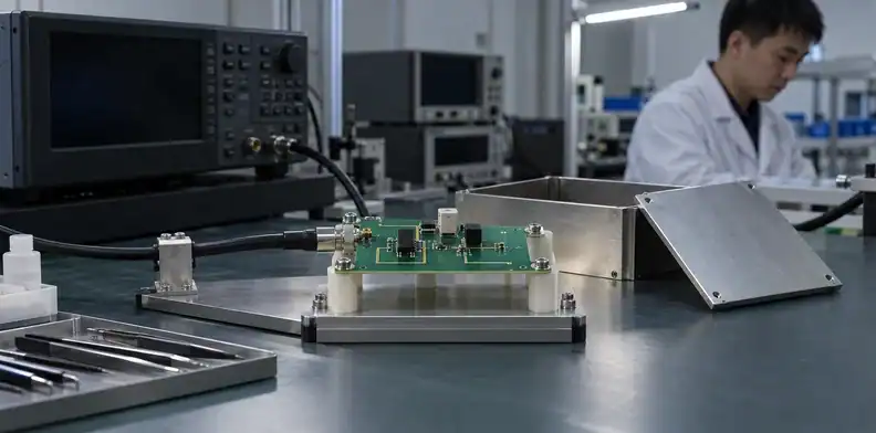
Measure the proposed circuit with a documented low-leakage fixture and operating sequence. A high-resolution instrument reading is meaningful only when the setup’s own contributions are understood.
Separate the board from fixture leakage
Define the input termination and reference state for the test. Characterize the fixture, cable and source configuration at the current scale being evaluated. A connector adaptor or probe assembly can add a path comparable to the board’s allowance.
Separate observations from inferred causes. An output offset can include amplifier bias, resistor effects and board leakage. Attribute a contribution only when the test method isolates it adequately. Keep the circuit’s calculated allowance beside the measured total error so a passing total is not mislabeled as a direct measurement of one parasitic path.
The first-article inspection scope can verify that the approved files and components were built. The low-current measurement supplies the electrical evidence for this guard application. Retain both when releasing the first assembly.
Exercise humidity, settling and input range
Record temperature, humidity, elapsed time after a stimulus change and the applicable input range. Select environmental conditions from the intended product use and qualification plan. There is no universal settling time or humidity threshold for all guarded boards.
For an illustrative sensor-buffer trial, examine several input levels within the valid range, then observe recovery after an agreed input change. For a biased TIA, use its actual reference and the prescribed sensor or input termination. Repeat relevant checks after coating or repair when those processes affect the sensitive region.
A time trace can distinguish a stable offset from a slowly settling measurement. Retain the trace and setup conditions when settling matters; a single favorable reading cannot explain the full behavior.
Send a guard-specific fabrication and assembly package
Release the guard net, geometry, exposed surfaces and handling requirements together with the circuit-specific test scope. This prevents a correct-looking ring from being built on the wrong net or processed under an unsuitable assumption.
| Package element | Guard-specific information | Reviewer |
|---|---|---|
| CAD and netlist | Sensitive net, guard net and driving source | Circuit/layout designer |
| Fabrication drawing | Layer coverage, exposed regions, material and finish | PCB engineering |
| Assembly notes | Paste exceptions, handling boundary and coating map | Manufacturing engineering |
| Test definition | Fixture, input state, environment, settling and allowance | Test/design engineering |
| Release record | Approved revision and resolved CAM deviations | Engineering and quality |
Highlight conflicts before release. A mask exception that contradicts the exported files, a guard called ground in the netlist or an unspecified driver jumper changes the intended construction. Resolve these details with the responsible engineer instead of letting production choose a default.
For recurring assemblies, identify the changes that trigger renewed verification: laminate, mask or coating changes; altered connector arrangements; replacement guard drivers; and repairs in the sensitive region. The test scope can then follow the relevant change instead of repeating unrelated work.
Provide QueenEMS with the guarded-region drawing and board data alongside the assembly and measurement requirements. A named guard net, local process boundary and interpretable test record give the quotation team concrete requirements to review.

Sources
Written by the QueenEMS Engineering Team
Upload your files today · Free DFM check before production · Ship worldwide
Get your PCB prototypes in as fast as 24 hours. We handle FR4, Rogers, and hybrid boards up to 40 layers in volume production, with advanced builds subject to engineering review — free prototypes for 2–4 layer FR-4 boards, no minimum order.
Just upload your Gerber + BOM — we source every part, assemble, and inspect (AOI + X‑Ray) so you don't have to chase suppliers. Boards ship in as fast as 24 hours.