
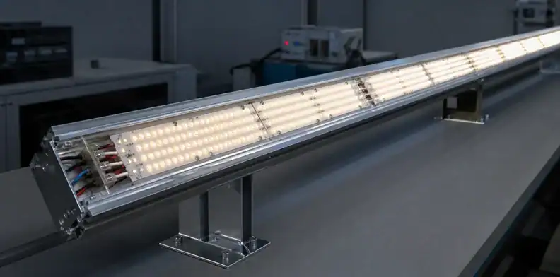
Quick Answer: A long LED PCB board needs voltage-drop control around the complete supply-and-return loop and a continuous thermal path into the final fixture. Use distributed feeds or local current regulation when one end feed cannot hold brightness. Validate electrical, optical and temperature results together on the installed assembly.
A one-meter lighting board can illuminate unevenly even when every LED and resistor matches the BOM. Copper resistance reduces voltage along the feed and return, local temperature changes LED forward voltage and light output, and the metal channel or luminaire may contact some regions better than others. Assembly adds another risk: a long narrow PCB can flex during printing, placement and reflow.
This article addresses long rigid lighting boards used in luminaires, industrial indicators, architectural systems and similar products. It does not replace LED-driver design or the general extra-long PCB manufacturing route. The design must bring electrical distribution, thermal paths, optical uniformity and assembly constraints together in one buildable LED board.
Table of Contents
- Define the lighting and mechanical requirement
- Calculate voltage drop through both conductors
- Choose feed and current-control architecture
- Build a continuous thermal path
- Decide between one long board and modules
- Design the board for stable assembly
- Validate light, temperature and reliability
- Release one correlated lighting baseline
- Prepare a long LED board quotation
Define the lighting and mechanical requirement
The PCB architecture should begin with measurable optical, electrical, thermal and mechanical requirements. “Uniform brightness” is not sufficient unless engineering defines the measurement distance, operating condition and allowed variation.
Translate optical intent into zones
Record luminous or irradiance targets, color consistency, LED spacing, diffuser distance, viewing geometry and the permitted end-to-end variation. Divide the length into zones that can be measured and compared. A diffuser can blend small point variations but cannot correct a large electrical gradient.
Identify whether the product is constant-current, constant-voltage or locally regulated. Include dimming method, maximum duty cycle and startup behavior. These choices control how supply variation becomes LED current and light output.
Capture the installed heat sink and support
Define the aluminum extrusion, housing, thermal interface material, fastener pattern, adhesive, airflow and mounting orientation. The PCB alone cannot be thermally qualified without the fixture that receives its heat. Mark contact gaps, screw bosses and connector locations on the mechanical model.
The same support drawing should show manufacturing rails or carriers. A board that is fully bonded in the product may still sag while bare or during reflow, so installation stiffness cannot be credited to every production step.
Include environmental and optical aging requirements that change the design baseline. Outdoor luminaires, sealed housings and high ambient equipment may run much hotter than an open bench sample. Diffuser yellowing, LED lumen maintenance and thermal-interface aging are product-level concerns, but the PCB validation plan should preserve the temperatures and current conditions needed for those assessments.
Calculate voltage drop through both conductors
Voltage drop must include the positive feed and return path, connector/contact resistance and the current drawn by downstream zones. Treating only one trace length understates the loop loss.
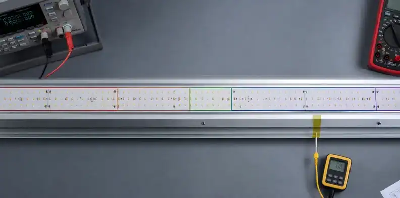
Build a segment model from copper resistivity, finished copper thickness, trace width, temperature and current. Current is highest near a single end feed because that section carries every downstream branch; it decreases after each LED group. Calculate node voltage and branch current along the board rather than applying one average current to the full length.
Consider an illustrative four-zone board. Each zone draws 0.25 A, and each segment from the feed to the first zone and between adjacent zones has 0.05 Ω of combined feed-and-return resistance at the evaluated temperature. Segment currents are 1.00, 0.75, 0.50 and 0.25 A. The far-end loop drop is 0.05 × (1.00 + 0.75 + 0.50 + 0.25) = 0.125 V. This assumes regulated zone currents and must be recalculated if a driver leaves regulation.
Subtract cable and connector losses as well, then compare the remaining local voltage with the LED string and driver headroom requirements. Infineon’s BCR430U application note relates minimum supply voltage, LED forward voltage and regulator margin to strip length. Its device values apply to that driver. Record the calculated node voltages beside each zone’s stabilized light and temperature measurements.
| Input | Why it matters | Release evidence |
|---|---|---|
| Supply voltage and tolerance | Sets headroom for strings/regulators | Worst-case power specification |
| LED forward-voltage range | Changes branch current and dropout margin | Approved LED data and bin plan |
| Branch current | Sets copper loss and heat | Schematic/current budget |
| Finished copper geometry | Determines loop resistance | Gerber plus copper requirement |
| Connector/contact resistance | Adds end or junction loss | Connector specification/test |
| Operating temperature | Raises copper resistance and shifts LED behavior | Thermal validation condition |
Use simulation or a spreadsheet for early design, then verify actual node voltages on a production-representative assembly at cold and stabilized temperature. The model should state acceptable voltage/current or light variation, not merely report millivolts.
Include the return conductor topology exactly as routed. Shared narrow returns can couple zones even when each positive feed looks adequate. Connector pins, vias, neck-downs near LEDs and transitions between copper widths deserve separate resistance entries. A thermal rise increases copper resistance, so the stabilized condition can show a larger end-to-end gradient than the initial cold measurement.
Document the calculation revision with schematic and layout data. A late change in LED count, branch current, copper thickness or feed cable can invalidate the result without changing the board outline. The purchasing drawing should not carry an unsupported voltage-drop promise that depends on an obsolete circuit model.
Evidence check: Verify modeled feed and return losses with measured node voltage on the stabilized first article.
Choose feed and current-control architecture
Power architecture should keep every zone inside its current-control headroom across supply, component and temperature tolerances. Increasing copper width can help, but it is only one option.
Compare end feed, center feed and distributed injection
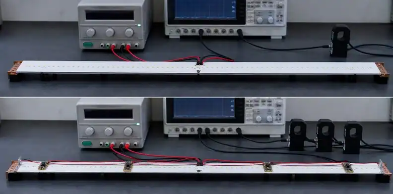
A single end feed is simple and may work for low current or short lengths. Center feed halves the maximum path for a symmetric load. Feeding both ends or adding distributed injection reduces conductor loss but requires connector, wiring and protection decisions so sources do not interact unpredictably.
Document feed-point identity and polarity. Long lighting products often use field connectors; reverse connection, uneven contact resistance and cable drop belong in the system calculation. Fuses or current limiting may be required by product engineering.
Choose resistor strings or local regulation deliberately
Constant-voltage resistor groups are simple but sensitive to supply and LED forward-voltage variation. Local constant-current devices can improve zone consistency when they retain enough dropout margin at the farthest point. Series-string architecture changes the voltage and fault behavior, while addressable LEDs add data integrity and power-distribution constraints.
Do not select the architecture from brightness alone. Review efficiency, fault containment, dimming, EMC, component availability, heat and service requirements. The PCB manufacturer should build the released circuit, not decide current-regulation strategy from a quotation note.
Build a continuous thermal path
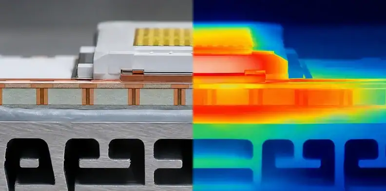
Thermal design must connect the LED junction to the installed ambient through package, solder pad, copper, dielectric, board, interface material and fixture. A low-resistance board cannot compensate for a poor contact surface or trapped air gap.
Spread heat without breaking electrical control
Use the LED manufacturer’s recommended land pattern and thermal pad. Copper spreading, thermal vias, thicker copper, metal-core construction or insulated metal substrate may reduce board-level thermal resistance where compatible with electrical isolation and fabrication.
Avoid assuming that more copper is always better. Large plane changes can affect solder-paste heating, copper balance, electrical segmentation and rework. Review current density and thermal spreading together.
Copper geometry must also preserve current-control separation between zones. A shared spreading plane may carry return current or couple heat into a driver region. Review electrical-net ownership and the board-to-fixture path together before enlarging pours or adding thermal vias, then verify the choice on the installed assembly.
Control the board-to-fixture interface
Specify flatness, surface cleanliness, thermal interface material, bond-line thickness, pressure and fastener/adhesive pattern. A long extrusion may have its own straightness and tolerance. Gaps create local hot zones even when board calculations appear uniform.
Measure representative case/board temperatures and use manufacturer thermal data to evaluate junction conditions. Infrared images are useful for locating patterns, but emissivity and reflective surfaces can distort absolute readings; correlate them with contact sensors where accuracy matters.
Decision point: Select feed architecture only after every zone retains current-control margin at worst-case supply.
Decide between one long board and modules
One long PCB reduces inter-board connectors and can simplify optical spacing, but it increases material, equipment, handling and replacement risk. Modules introduce joints and wiring while improving panel utilization, assembly access and field service.
Compare the product at system level:
| Decision area | One long board | Repeated modules |
|---|---|---|
| Optical spacing | Continuous datum across length | Joint gap requires control |
| Power distribution | Long copper loop | Feeds can be distributed per module |
| Fabrication/assembly | Special large-format route | Standardized smaller route may fit |
| Connectors/wiring | Fewer internal joints | Added contact loss and assembly work |
| Repair | Large replacement unit | Failed segment may be replaceable |
| Thermal contact | One continuous interface to qualify | Repeated interface tolerances |
The existing one large PCB versus multiple boards comparison provides the wider architecture framework. For lighting, add diffuser seam, zone current, color/brightness calibration and thermal contact at every joint.
Design the board for stable assembly
Long narrow LED boards need repeatable support through paste printing, placement, reflow, depaneling and handling. Electrical simplicity does not make the mechanical route simple.
Support the active print and placement area
Provide tooling edges, fiducials and support zones that do not collide with bottom-side features. The stencil printer must maintain gasket contact along the full length; placement needs camera/gantry access and a stable coordinate system. Split printing or multiple placement passes require explicit re-registration and inspection.
Use the oversized PCB solder-paste printing review when one pass is not possible. LED apertures and thermal-pad deposits should follow component/paste engineering rather than a generic large-board pattern.
Control reflow and post-process shape
Profile hot, cold and sensitive zones on the populated board with the production carrier/orientation. Repeated LEDs may look thermally uniform, but connectors, drivers, large copper feeds and fixture contact create local differences.
Design carrier supports to avoid LED lenses and solder joints. After reflow, measure flatness in the condition required for fixture contact. A board that screws flat only under high force can create local stress or a variable thermal interface.
For a contextual buildability check, compare the board outline, LED/driver BOM, power map, support zones and housing model against this PCB DFM review workflow. The manufacturing disposition should cover board-size feasibility, printing, placement, reflow support and inspection access.
Thermal rule: Approve the board only with the real interface material, fixture contact and operating power represented.
Validate light, temperature and reliability
Validation should compare electrical, optical and thermal results under the same controlled operating conditions. Measure input voltage/current, zone node voltage, branch current where practical, light output or illuminance, color metric required by the product and representative temperatures after stabilization.
Test cold start, nominal steady state, maximum allowed ambient or enclosed condition, dimming extremes and supply tolerance selected by product engineering. Map results by zone so a far-end electrical drop can be distinguished from a local thermal-contact problem or LED-bin variation.
Inspect solder joints, LED alignment, board shape, fixture contact and connector heating. Reliability testing follows the application: thermal cycling, power cycling, vibration, humidity or burn-in may be required. Do not invent a universal duration; use customer, regulatory and component requirements.
Create a golden dataset rather than relying only on a visual golden sample. Store board/BOM/firmware revision, LED bin, fixture, supply settings, optical setup, sensor positions, ambient, results and acceptance. Future substitutions or mechanical changes can then be reviewed against the same baseline.
Repeat measurements after thermal stabilization at several positions along the fixture. A single lux-meter reading at the center can miss an end gradient, and one thermocouple beside the driver can miss poor contact beneath a remote LED zone. Use the same geometric setup, diffuser state and warm-up definition for every comparison.
Fault behavior belongs in the plan as well. An open LED, shorted branch, loose feed or high-resistance connector can redistribute current and heat. Verify that protection and diagnostics respond as intended without allowing a local hot spot to damage the long board or housing.
Release one correlated lighting baseline
The final decision should connect electrical, thermal, optical and mechanical results from the same controlled assembly condition.
| Evidence group | Baseline record |
|---|---|
| Product configuration | Board, BOM, LED-bin and driver or firmware revisions |
| Electrical operating point | Supply voltage, feed topology, current and stabilized operating time |
| Installed state | Fixture, diffuser, interface material and fastening condition |
| Optical and thermal result | Measurement grid, acceptance result, sensor locations, ambient and stabilized readings |
| Manufacturing condition | Zone voltage/current data, flatness, solder-joint and connector inspection evidence |
Archive these records under one revision-controlled baseline rather than separating them into unrelated test folders.
If one domain is measured on a different build or fixture, identify the limitation and obtain engineering disposition. Otherwise a cold optical test, a separate thermal sample and an unrestrained dimensional check may each pass while no production-representative unit proves all requirements together.
Baseline rule: Release the lighting design only when the correlated dataset traces to one defined product and fixture state.
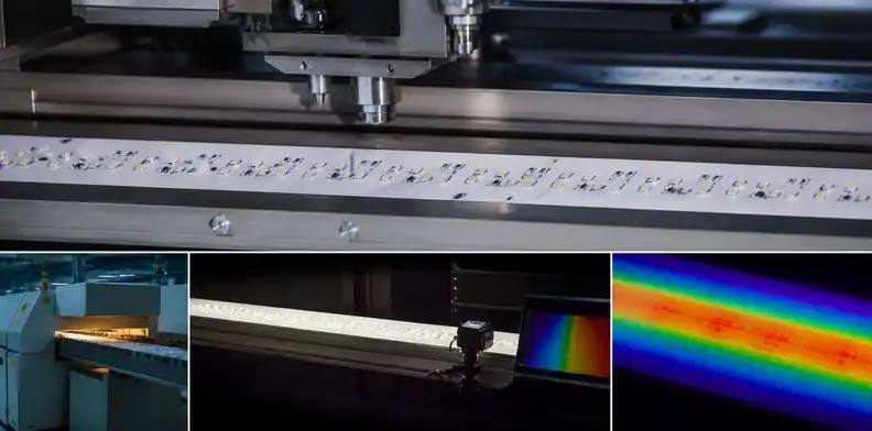
Prepare a long LED board quotation
The quotation package must let the supplier evaluate both the electrical design and the unusual production route. Provide the manufacturing artwork or ODB++ dataset, NC drill data, stack-up, material and copper requirements, finished outline/tolerance, BOM/AVL, centroid, assembly drawings, LED orientation/bin rules, solder-paste requirement, housing/contact model, quantity and test scope.
Add the power-distribution diagram with feed points, maximum current and connector definitions. Identify flatness/contact requirements, tooling edges, carrier expectations, acceptable panel joints or module options and required optical/thermal evidence. Separate customer-owned lighting performance from supplier-owned manufacturing checks.
For comparison quotes, require suppliers to name the assumed production panel, board orientation, stencil/placement route and test duration. A low board price may exclude the carrier, optical fixture or stabilized thermal run that the specification needs. Keep those items visible so purchasing can compare complete delivered evidence instead of unit price alone.
Quotation request: Deliver the complete lighting-board and fixture package with the QueenEMS long-board enquiry. The route-qualified response should state fabrication and assembly orientation, carrier or panel assumptions, first-article electrical/thermal checks and unresolved constraints.
Release rule: Optical uniformity, electrical margin and temperature must pass in the same controlled setup.
FAQ
Why are LEDs dimmer at the far end of a long PCB?
Voltage loss in feed and return copper, connector resistance and limited regulator headroom can reduce downstream current. Measure node voltage and current at operating temperature before attributing the difference only to LED bins.
Is thicker copper enough to fix brightness variation?
Not always. Wider/thicker copper reduces conductor loss, but feed architecture, driver regulation, connector resistance, supply tolerance and temperature may still control the result.
Should I power a long LED board from both ends?
Use dual-end or distributed feeds when the calculated loop drop and regulation margin require them, with protection and wiring designed so supplies cannot interact unsafely. Product engineering owns that circuit decision.
Is aluminum-core PCB always required for LEDs?
No. Board technology depends on LED power density, copper spreading, electrical isolation, fixture contact, ambient and allowable temperature. FR-4 may fit lower-power designs; metal-core or another thermal structure may fit higher heat flux.
Is one long LED PCB cheaper than several modules?
Not automatically. Compare material utilization, special equipment, carriers, connectors, wiring, assembly, test, replacement and optical/thermal joint control across the complete product.
Sources
- ams OSRAM AN052: Thermal Management of LED Light Sources
- Cree LED: Optimizing PCB Thermal Performance for XLamp LEDs
Written by the QueenEMS Engineering Team
Upload your files today · Free DFM check before production · Ship worldwide
Get your PCB prototypes in as fast as 24 hours. We handle FR4, Rogers, and hybrid boards up to 40 layers in volume production, with advanced builds subject to engineering review — free prototypes for 2–4 layer FR-4 boards, no minimum order.
Just upload your Gerber + BOM — we source every part, assemble, and inspect (AOI + X‑Ray) so you don't have to chase suppliers. Boards ship in as fast as 24 hours.