Quality · inspection · DFM · standards
PCB Capabilities: Fabrication, Assembly, Inspection & Certifications
Everything we can build, test and document in our Shenzhen factory, on one page. Check your board against our PCB manufacturing and assembly capabilities, see which inspection methods it needs, and send it for a free DFM review before you order.
Will we build it?
Check Your Board in Seconds
Pick your board’s key parameters. The checker compares them with our published limits and tells you whether it is a standard build, needs engineering review, or falls outside what we make.
Your check result is attached to the message automatically. Prefer email? Use our contact page.
Fabrication
PCB Manufacturing Capabilities at a Glance
The key limits for bare boards. Board-type pages and the full capability table on our PCB manufacturing page list every parameter.
| Parameter | Capability | Details |
|---|---|---|
| Layer count | Standard up to 24; advanced up to 100 | Multilayer PCB |
| Board thickness | 0.15–10.0 mm | |
| Max panel size | 22.5″ × 48″ (572 × 1219 mm) | Large format PCB |
| Min line / space | 3/3 mil (75 µm); 6/8 mil at 3 oz; 9/14 mil at 6 oz+ | |
| Min mechanical drill | 0.10 mm (4 mil) | |
| Laser microvia | 0.075 mm (3 mil); stacked and staggered | HDI PCB |
| Aspect ratio | Up to 20:1 | |
| Copper weight | Inner 0.5–12 oz; outer 0.5–28 oz | Heavy copper PCB |
| Impedance control | ±5%, verified by TDR | Impedance calculator |
| Surface finish | ENIG, ENEPIG, OSP, HASL; hard gold fingers | |
| Flex / rigid-flex | Flex 1–8 layers; rigid-flex 4–20 layers | Flexible PCB |
| Acceptance standard | IPC-6012 / IPC-A-600, Class 2 or 3 |
Upper limits are available for prototypes and engineering builds; for production volumes we confirm them case by case. See the full PCB manufacturing capability table →
Assembly
PCB Assembly Capabilities
Boards fabricated in our factory can be assembled on our own SMT lines, so one team owns the result from bare board to finished assembly.
| Parameter | Capability | Details |
|---|---|---|
| Component size | 01005 up to 100 mm parts | SMT assembly |
| BGA pitch | Down to 0.3 mm | BGA assembly |
| Placement speed | Up to 90,000 components per hour | |
| Assembly types | SMT, through-hole and mixed technology | Through-hole · Mixed assembly |
| Programming | IC programming and testing | IC programming & testing |
| Inspection | 3D AOI and X-ray | Inspection methods |
| Acceptance standard | IPC-A-610, Class 2 or 3 | |
| Quantity | From 1 piece for prototype assembly | Quick-turn assembly |
Inspection & test
PCB Quality Control and Inspection
AOI, X-ray, flying probe, ICT and functional test all run in our own factory. Which ones your order gets depends on volume, hidden joints, IPC class and test-point access.
| Method | What it catches | When we use it |
|---|---|---|
| Electrical test | Opens and shorts on every net of the bare board | 100% of bare boards, before shipment or assembly |
| AOI | Inner-layer defects before lamination; on assemblies, missing, shifted or reversed parts and solder fillets (3D AOI) | Every inner layer and every assembled board |
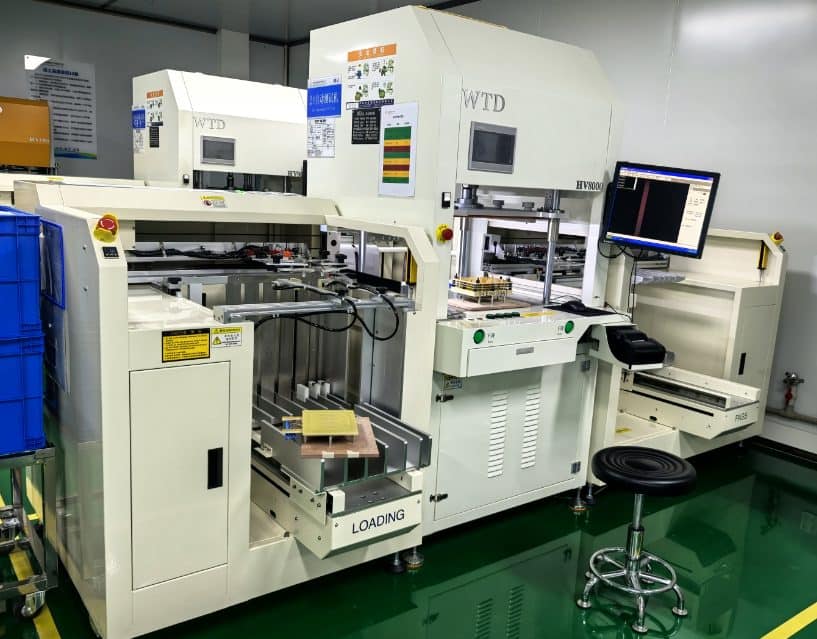
| X-ray | Voids, bridges and opens under BGA, QFN and other hidden joints | Boards with BGA or QFN; 100% for dense BGA or Class 3 |
| Flying probe | Shorts, opens and component values without a fixture | Prototypes, low volumes, or layouts without test points |
| ICT | Shorts, opens and component values through a bed-of-nails fixture | Mid and high volumes with accessible test points |
| Functional test | Whether the powered board works as designed | To your test specification; recommended for Class 3 |
| XRF thickness | Nickel and gold thickness on ENIG | Every lot; readings available on request |
| Impedance (TDR) | Controlled-impedance traces within ±5% | Boards with impedance requirements |
| Solderability | Whether bare-board pads wet properly | In-house test on bare boards |
- Incoming checkLaminates and components checked against the order, including full part numbers.
- In-processInner-layer AOI before lamination; XRF on ENIG; impedance coupons where specified.
- Final test100% electrical test on bare boards; AOI, X-ray and electrical or functional test on assemblies.
- DocumentsInspection results ship with your boards. See a sample QC report.
Plan your inspection
Which Inspection Methods Does Your Board Need?
Answer four questions to get a recommended mix. A full guide to each method explains the trade-offs.
Certifications
Certifications and Standards
Bare boards are built to IPC-6012 and inspected to IPC-A-600; assemblies are inspected to IPC-A-610. The class on your order sets the limits.
| Class 2 | Class 3 | |
|---|---|---|
| Typical products | Industrial, telecom, consumer electronics | Medical, aerospace and other high-reliability products |
| Bare board | Standard plating and annular ring limits | Tighter limits; hole wall copper ≥25 µm |
| Inspection | X-ray by sampling for BGA | 100% X-ray for BGA; functional test recommended |
More detail: IPC Class 2 vs Class 3 PCB.
Engineering review
DFM Review Before Anything Is Built
More than 20 CAM engineers check your Gerber or ODB++ data, drill files and stack-up notes against our limits before production. Problems are flagged before you pay for a board.
- Free PCB DFM checkUpload your files and get manufacturability issues flagged before quoting.
- PCB DFM case studyWhat a DFM review found on a real board, and what changed.
- Trace width and impedance calculatorsCheck trace geometry before you send files.
- PCB material selectorCompare laminates by Dk, Df and Tg.
Ordering
Quotes, Lead Times and Quantities
Within 2 hours of receiving complete files, Mon–Sat 9AM–6PM CST.
Within 24 hours.
2–4 layer FR-4 prototypes are free for new customers.
No minimum order. Prototypes start from 1 piece.
Reference lead times by layer count and board area are on our home page; your quote confirms the ship date.
We build to the panel drawing you supply.
Quality guides
PCB Quality and Acceptance Guides
What to specify, inspect and ask for on a PCB order.
Inspection & testing
Acceptance criteria
Standards & certification
FAQ
PCB Capabilities FAQ
What are Queen EMS’s PCB manufacturing capabilities?
Standard builds go up to 24 layers and advanced builds up to 100 layers, with 3/3 mil line/space, 0.10 mm mechanical drills, 0.075 mm laser microvias, 0.15–10.0 mm thickness and copper up to 28 oz. The full table is on our PCB manufacturing page.
What PCB assembly capabilities do you have?
We place components from 01005 up to 100 mm, BGAs down to 0.3 mm pitch, at up to 90,000 components per hour, and inspect to IPC-A-610 Class 2 or Class 3. See SMT assembly.
Which inspection and test methods do you use?
Every bare board is 100% electrically tested. Assembled boards go through 3D AOI, X-ray for BGA and QFN joints, flying probe or ICT, and functional test when specified. Use the inspection method selector to see which mix fits your board.
Can you build to IPC Class 3?
Yes. Bare boards are built and inspected to IPC-6012 / IPC-A-600 Class 2 or Class 3, and assemblies to IPC-A-610 Class 2 or Class 3, as specified on your order.
Which certifications does Queen EMS hold?
ISO 9001:2015, ISO 14001:2015 and ISO 45001:2018, plus UL file E518360 for printed wiring boards. RoHS and REACH compliance is supported by SGS test reports.
Are the upper limits available for production orders?
The upper limits (100 layers, 28 oz copper, 0.10 mm drills, 20:1 aspect ratio) are available for prototypes and engineering builds. For production volumes we confirm them case by case during DFM review.
How do I check whether my board fits your capabilities?
Use the Capability Quick-Check above for a fast read, or send your Gerber files for a free DFM check. Bare-board quotes come back within 2 hours.
Send Your Files for a Capability Review
A CAM engineer checks your board against these limits and returns a bare-board quote within 2 hours during business hours.