
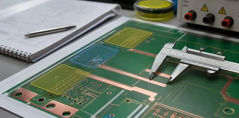
Quick Answer: High voltage PCB design should not start from a copied creepage table. Before RFQ, define the working voltage, transient overvoltage category, pollution degree, altitude, CTI material group, coating or potting plan, slot strategy, copper-to-edge rule, test evidence, and certification owner. IEC 60664-1 is the usual insulation-coordination reference, but the final spacing must be confirmed against the product safety standard and the actual use environment.
Key takeaways
- Creepage and clearance are different risks; do not use one number for both.
- CTI, pollution degree, altitude, coating, and slots can change the required spacing.
- Example values can guide RFQ planning, but they are not certification approval.
- Ask the PCB supplier what it can manufacture and ask the safety owner what the product must pass.
Table of Contents
- Start with the safety standard, not the PCB drawing
- Separate clearance from creepage before quoting
- Collect voltage, pollution degree, CTI, and altitude inputs
- Use slots, coating, and barriers only with approval
- Connect spacing to copper edge and fabrication limits
- Ask for manufacturable evidence before release
- Write a high-voltage RFQ note that avoids false certainty
Start with the safety standard, not the PCB drawing
The most dangerous high-voltage PCB mistake is pretending that the PCB supplier alone can decide the spacing. A fabricator can tell you what gap, slot, copper clearance, mask opening, and material it can manufacture. It cannot certify the end product unless it is also responsible for the safety design and test program. The buyer needs a product-level standard owner before the PCB RFQ becomes final.
Safety call: Treat high-voltage PCB spacing as a product safety decision first and a fabrication rule second.
Many AI answers give a quick creepage or clearance number for 400V, 800V, or 1,000V. That feels useful, but it can hide the variables that matter. IEC 60664-1 deals with insulation coordination for equipment in low-voltage systems up to 1,000 V AC or 1,500 V DC. It considers rated voltage, impulse voltage, pollution degree, material group, and other conditions. Product standards for EV chargers, solar inverters, industrial drives, medical equipment, or appliances may add their own requirements.
For QueenEMS, the safer RFQ question is not “what spacing do you recommend?” It is “here are the product standard, working voltage, pollution degree, CTI material group, coating plan, altitude, and required test evidence; can you build this PCB and what drawing notes do you need?” That turns a vague high-voltage request into a quote-ready engineering package.
This article is therefore written for purchasing owners, engineers, and founders who need to prepare a supplier RFQ. It is not a substitute for product safety certification. If the certification owner has not approved the spacing philosophy, the PCB order is not ready for production release.
Separate clearance from creepage before quoting
Clearance is the shortest distance through air between conductive parts. Creepage is the shortest distance along an insulating surface. They solve different problems. Clearance is mainly about arcing through air. Creepage is mainly about surface tracking, contamination, humidity, and insulation material behavior. A high-voltage board can meet one requirement and fail the other.
Spacing rule: Ask for both clearance and creepage values; a single “high-voltage gap” is not enough.
This distinction matters in PCB layout. Two copper features may have a direct air gap of 3.0 mm, but the creepage path along the board surface may be longer or shorter depending on slots, solder mask, board edge, coating, and nearby copper. A routed slot can increase creepage path if it is designed and accepted correctly. A solder-mask opening can reduce the effective surface protection. A sharp copper corner can create field concentration even when the nominal spacing looks acceptable.
For RFQ purposes, draw the risky areas. Mark primary-to-secondary isolation, high-voltage bus to low-voltage control, relay contact gaps, connector pin spacing, transformer pins, optocoupler areas, and board-edge copper. If a supplier only sees Gerbers, it may fabricate the gap without understanding why the gap exists.
| Spacing term | What it protects against | Buyer RFQ question |
|---|---|---|
| Clearance | Air breakdown and transient stress | What minimum air gap must be held after fabrication tolerance? |
| Creepage | Surface tracking across insulation | What material group, pollution degree, and surface path apply? |
| Slot or cutout | Longer path or isolation improvement | Is the slot approved by the safety owner and manufacturable? |
| Coating or potting | Environmental control | Does the product standard allow reduction, and how is it inspected? |
This also links to PCB copper-to-edge clearance. High-voltage spacing is not only between two internal nets. Copper near the board edge can reduce the real insulation margin if the edge is exposed, rough, contaminated, or close to a metal enclosure.
Collect voltage, pollution degree, CTI, and altitude inputs
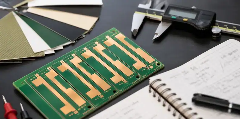
A high-voltage PCB quote should list the inputs that change spacing. The working voltage is only one input. The transient overvoltage category, pollution degree, material group, CTI value, altitude, coating plan, and insulation type can all change the requirement. A board designed for a clean indoor sealed product may not use the same assumptions as a board used outdoors near dust, moisture, and conductive contamination.
Input check: If the RFQ does not name pollution degree and CTI material group, the spacing request is not fully defined.
CTI, or comparative tracking index, describes how insulation material resists tracking under contamination. IEC-style material groups are often discussed as Group I, II, IIIa, and IIIb based on CTI ranges. A common planning example is CTI 600 or higher for Group I, CTI 400 to 599 for Group II, CTI 175 to 399 for Group IIIa, and CTI 100 to 174 for Group IIIb. The final group must come from the laminate data and safety review, not from the marketing name of the board.
Altitude also matters. Many standard clearances assume operation up to about 2,000 m. Above that, air is thinner and clearance may need correction. Pollution degree matters as well: Pollution Degree 2 is common for many controlled indoor electronics, while harsher environments may require different assumptions.
Use a planning record like this:
| RFQ input | Example planning entry | Who should confirm |
|---|---|---|
| Working voltage | 400 V DC, 800 V DC, or another actual value | Design engineer |
| Transient/impulse condition | Product-standard overvoltage category | Safety/certification owner |
| Pollution degree | PD2 for controlled indoor use, if approved | Safety/certification owner |
| CTI / material group | CTI value from laminate data sheet | PCB supplier and safety owner |
| Altitude | Up to 2,000 m or higher-altitude correction | Product owner |
For EV charger or solar designs, connect these inputs to the real service environment. An EV charger PCB assembly or solar inverter PCB assembly project can face different insulation, thermal, humidity, enclosure, and field-service expectations from a small indoor consumer device.
Use slots, coating, and barriers only with approval
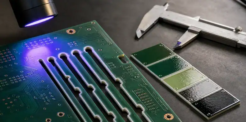
Slots are often proposed when the PCB does not have enough surface distance. A routed slot can lengthen creepage path, separate high-voltage zones, and give the designer more layout flexibility. Coating and potting can also control the environment around the board. These are useful tools, but they are not automatic shortcuts.
Approval point: Slots, coating, and barriers should reduce risk only when the applicable standard and inspection plan recognize them.
A slot must be wide enough and clean enough to manufacture repeatably. If the slot is plated, unplated, routed, punched, or laser-cut, the drawing should state the requirement. If the slot sits near copper, solder mask, or a component body, ask whether manufacturing tolerance can reduce the real path. If coating is used, ask how thickness, coverage, bubbles, masking, and inspection will be controlled.
This is where PCB plated slots and controlled routing rules become practical. A designer may draw a perfect isolation slot. A fabricator must produce it with tool diameter, registration tolerance, burr control, and cleanliness. A buyer should not assume that every CAM change keeps the safety path intact.
For high-voltage boards, a slot is not only a shape. It is a safety feature. The RFQ should say whether the slot is part of creepage, whether its wall can be exposed FR-4, whether coating must enter the slot, and whether inspection photos or first-article checks are required.
Connect spacing to copper edge and fabrication limits
High-voltage spacing can fail in boring ways. Copper can be too close to a routed edge. Solder mask can open more than expected. Silkscreen or contamination can appear where the board needs clean insulation. Drill tolerance can move a plated hole closer to a high-voltage net. Panel tabs can leave a rough edge near a safety gap. These are not theoretical problems; they are ordinary fabrication details that become serious at high voltage.
Fabrication signal: The safety spacing must survive PCB fabrication tolerance, not only ideal CAD geometry.
Ask for finished-copper-to-copper spacing, copper-to-edge spacing, slot tolerance, mask clearance, drill tolerance, and routing tolerance. If the required clearance is 3.0 mm on the drawing but fabrication tolerance can reduce it, the design may need a larger nominal value. If a board edge is part of the insulation boundary, ask whether the board will be routed smooth, whether fibers or burrs are acceptable, and whether the panelization method changes the edge.
For ceramic or metal-core power designs, the insulation path may involve material choices beyond ordinary FR-4. If the design is for 800V-class EV power electronics, review material choice with articles such as ceramic PCB for EV 800V power electronics rather than treating spacing as the only answer.
The purchasing lesson is simple: high-voltage design is not only a layout note. It is stackup, material, routing, slotting, cleaning, coating, inspection, and certification evidence working together. A quote that does not mention these assumptions is not fully comparable.
Ask for manufacturable evidence before release
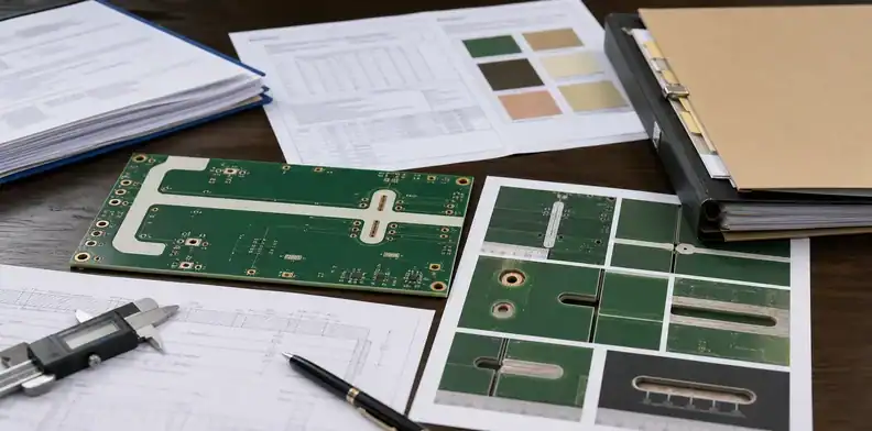
Before production release, ask the PCB supplier for evidence that matches the risk. For a prototype, a DFM response and first-article inspection may be enough. For a higher-risk production board, ask for material certification, CTI or material group statement, slot and routing inspection, finished spacing checks, solder-mask review, and any test coupons required by the product owner.
Evidence check: A supplier answer is useful only when it proves the specific high-voltage assumption that the buyer is relying on.
Do not ask for a generic quality certificate and assume it covers high-voltage spacing. Ask for the item that matters. If the design relies on CTI, get laminate evidence. If the design relies on a slot, get slot dimension and location evidence. If the design relies on coating, get coating process and inspection evidence. If the design relies on finished spacing, get measurement from the finished board, not only the CAD file.
| Risk being controlled | Useful evidence | Weak evidence |
|---|---|---|
| CTI / material group | Laminate data or approved material declaration | “FR-4 high quality” wording |
| Clearance after routing | Finished-board measurement | CAD screenshot only |
| Creepage slot | Slot width, position, burr review | Uncontrolled CAM promise |
| Coating support | Coating process and inspection plan | Generic coating statement |
QueenEMS can help review the quote package before the supplier starts production. If the product owner has not chosen the safety standard, we will flag that as an open decision instead of pretending the PCB factory can solve it alone.
Write a high-voltage RFQ note that avoids false certainty
A good RFQ note is precise without pretending to certify the product. It should say the product standard or safety owner controls final spacing, then list the spacing assumptions the PCB supplier must support. It should also define hold points: when the supplier must ask before changing material, slot geometry, copper clearance, coating, or panelization.
RFQ record: The supplier should quote what will actually be built, and the safety owner should approve what the product must pass.
Practical wording can be:
“High-voltage spacing is controlled by the customer safety review. Supplier to fabricate per released drawing and confirm finished clearance, creepage-related slots, copper-to-edge rules, laminate material group / CTI evidence, and routing tolerance. Do not change laminate, slot geometry, coating assumption, copper spacing, or panelization near high-voltage areas without written approval.”
This wording does not give a magic number. It creates a controlled quote record. It also gives purchasing a way to compare suppliers. A low quote that ignores CTI, slots, and finished spacing is not equal to a quote that includes high-voltage evidence.
For PCB and PCBA orders, send the same high-voltage assumptions with the assembly files. Connector selection, creepage across component bodies, coating after assembly, cleaning residues, and test fixtures can all affect the final product. A PCB-only quote may miss those issues if the assembler does not see the full context.
FAQ
Can I use one creepage table for every high-voltage PCB?
No. Creepage depends on voltage, pollution degree, material group, CTI, environment, coating, and the product safety standard. A table can help planning, but it is not final certification approval.
Is 800V always the same spacing requirement?
No. An 800V DC design in a clean sealed indoor environment can have different assumptions from an outdoor, high-altitude, contaminated, or safety-critical product. The final rule must come from the applicable standard and certification owner.
Do slots always reduce creepage risk?
Slots can help when they are accepted by the safety approach and manufactured correctly. A poorly defined slot can also create inspection and tolerance risk. Treat slots as controlled safety features.
What should QueenEMS review before quoting?
Send the schematic isolation areas, PCB layout, voltage levels, expected product standard, pollution degree, altitude, CTI requirement, coating or potting plan, slot drawings, and assembly constraints. QueenEMS can help convert those inputs into a quote-ready high voltage PCB design package.
Related QueenEMS articles
- EV Charger PCB Assembly
- Solar Inverter PCB Assembly
- PCB Copper-to-Edge Clearance Requirements
- PCB Plated Slots Requirements
- Ceramic PCB for EV 800V Power Electronics
If your PCB or PCBA project has high-voltage isolation, EV charger, solar inverter, power supply, or industrial control requirements, send QueenEMS the released files and safety assumptions. We can help review manufacturability, supplier evidence, assembly constraints, and RFQ hold points before production starts.
Written by the QueenEMS Engineering Team
Sources
- IEC, IEC 60664-1 insulation coordination standard page: https://webstore.iec.ch/publication/67383
- UL Standards & Engagement, UL 840 insulation coordination standard page: https://www.shopulstandards.com/ProductDetail.aspx?productId=UL840
Upload your files today · Free DFM check before production · Ship worldwide
Get your PCB prototypes in as fast as 24 hours. We handle FR4, Rogers, and Flex up to 60 layers — free prototypes for 2–4 layer boards, no minimum order.
Just upload your Gerber + BOM — we source every part, assemble, and inspect (AOI + X‑Ray) so you don't have to chase suppliers. Boards ship in as fast as 24 hours.