
For PCB designers pushing the limits of miniaturization, navigating the transition from conventional High-Density Interconnect (HDI) to Any-Layer ELIC (Every Layer Interconnect) is a notorious bottleneck. While any-layer stackups promise absolute routing freedom by allowing microvias to be stacked and routed on every single layer, they come with a substantial cost premium and highly restricted manufacturing avenues.
From a factory engineer’s perspective, this guide provides a concrete decision framework. We will analyze when the premium of ELIC is technically mandatory, when a more cost-effective sequential lamination build (like 2+N+2) is perfectly sufficient, and the yield and registration tolerances that dictate these real-world factory economics.
Table of Contents
- 1. What Is HDI Any-Layer (ELIC) vs Sequential Lamination?
- 2. When Should You Choose ELIC Over Sequential Lamination?
- 3. How Much More Does ELIC Cost Than 2+N+2 Sequential Lamination?
- 4. Which Fabs Can Actually Build True Any-Layer HDI Reliably?
- 5. What Are the Yield Differences Between ELIC and Sequential Lamination?
- 6. How Does Lamination Cycle Count Affect HDI Cost and Reliability?
- 7. What Materials Work Best for ELIC vs Sequential Lamination?
- 8. How Do Microvia Stack Requirements Differ Between Build Types?
- 9. What Applications Truly Require ELIC vs Traditional HDI?
- 10. How Do You Specify HDI Build Type in Your Fabrication Notes?
- Frequently Asked Questions (FAQ)
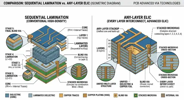
1. What Is HDI Any-Layer (ELIC) vs Sequential Lamination?
To understand the core manufacturing differences, we must start with the baseline industry standards defined in IPC-2226A Sectional Design Standard for High Density Interconnect (HDI) Printed Boards. Under IPC-2226A, high-density structures are classified into different build types based on how many sequential lamination cycles are required to achieve the routing density.
- Sequential Lamination (Type I, II, and III): This traditional HDI process starts with a standard cured core (the “N” layers). Additional layers are laminated sequentially, adding microvias to connect outer layers to the inner core. These are typically designated as 1+N+1, 2+N+2, or 3+N+3 builds. For example, a 2+N+2 stackup requires two sequential lamination cycles to build up the blind/buried microvias on the outer layers.
- Any-Layer ELIC (Every Layer Interconnect): In a true ELIC build, there is no conventional core. Instead, every single dielectric layer is drilled with microvias, filled completely with electroplated copper, and laminated sequentially. This structure creates a continuous, vertical, solid-copper column of stacked microvias that can route signals freely from layer 1 to layer X.
The physical difference is routing density. While sequential lamination relies on staggered microvias or limited stacked layers over a core, ELIC allows every layer to act as an interconnect junction, saving up to 40% of the horizontal board area.
Table 1: Build Type Comparison Matrix
| Build Type | Typical Layer Count | Cost Factor | Lamination Cycles | Fab Availability | Typical Applications |
|---|---|---|---|---|---|
| 1+N+1 (Type I / II) | 4 – 8 | 1.0x (Baseline) | 1 | Excellent (over 95% of fabs) | Entry-level smart devices, IoT nodes, automotive dashboards |
| 2+N+2 (Type III) | 6 – 12 | 1.4x – 1.6x | 2 | Very Good (around 75% of fabs) | Consumer wearables, mid-range smartphones, standard ADAS |
| 3+N+3 (Type III Advanced) | 8 – 16 | 1.8x – 2.0x | 3 | Moderate (around 30% of fabs) | High-end medical imaging, network switches, rugged military boards |
| Any-Layer ELIC | 8 – 18 | 2.2x – 2.5x | N-1 | Very Low (under 20 fabs globally) | Flagship smartphones, HBM3/AI GPU accelerator cards, dense SiP |
2. When Should You Choose ELIC Over Sequential Lamination?
As an engineer on the factory floor, the most common question I see on design forums like r/PrintedCircuitBoard is: “Do I really need ELIC for my design, or can 2+N+2 work? My board has a 0.5mm pitch BGA with 1024 balls and 8 high-speed differential pairs.”
The answer depends on a strict physical threshold: BGA pitch, total I/O count, and board thickness constraints.
If you are dealing with a 0.5mm pitch BGA with fewer than 1000 balls, you do not need ELIC. With a smart HDI stackup type comparison, a standard 2+N+2 stackup combined with routing optimization (such as utilizing via-in-pad and narrow trace geometries) is more than enough to escape-route your design.
However, you must choose ELIC under the following critical threshold:
- The BGA pitch is 0.4mm or less with an I/O count exceeding 1500 pins.
- Your layout contains more than 8-12 high-speed differential pairs that must navigate extremely cramped routing channels in a Z-axis constrained design (e.g., thickness of 0.8mm or less).
- The board must support massive parallel busses (like HBM3 memory routing) next to high-performance SoCs.
Forcing a 2+N+2 sequential build on a 0.4mm pitch, 1500-pin BGA usually fails DFM because staggered microvias require too much lateral real estate, blocking escape channels. Shifting to ELIC will add roughly 300 to 500 dollars per board in base fabrication costs at low volumes, but it is often the only mathematically viable way to execute the escape routing.
3. How Much More Does ELIC Cost Than 2+N+2 Sequential Lamination?
If your design crosses the threshold into ELIC, you must prepare for a significant cost increase. A question frequently raised on the EEVBlog Forum asks: “Why does ELIC cost so much more — is it the microvias themselves or the lamination process?”
The primary cost driver in ELIC is not the physical action of laser drilling. Laser drilling itself only contributes about 15% to the cost increase. The real-world cost premium of any-layer HDI is driven by three distinct process factors:
- Solid Copper-Fill Electroplating (~25% of cost): Every microvia on every layer of an ELIC board must be completely filled with copper to allow the next layer’s microvia to stack directly on top of it. This requires specialized plating lines with low-dimple chemistry (5 microns or less dimple control) and incredibly long plating dwell times.
- Lamination Cycles & Equipment Time (~30% of cost): An N-layer ELIC board requires N-1 lamination cycles. A 12-layer ELIC board requires 11 vacuum lamination press cycles. In comparison, a 12-layer 2+N+2 board requires only 3 lamination cycles. This ties up the factory’s primary heavy machinery for days.
- Yield Buffer (~20% of cost): Because any-layer HDI is a high-risk fabrication process, factories build a 20% yield insurance buffer directly into the per-panel pricing.
At a 12-layer count, the final cost multiplier of an ELIC build is approximately 2.2x that of a comparable 2+N+2 sequential lamination build, and roughly 1.5x that of a 3+N+3 build. Every additional pair of stacked microvia layers added to a conventional sequential design adds roughly 15 to 25 dollars per panel in raw processing costs.
4. Which Fabs Can Actually Build True Any-Layer HDI Reliably?
When sourcing suppliers, designers must be cautious of marketing exaggeration. This EEX Stack Exchange post captures a very real frustration: “Which fabs in China can actually deliver reliable ELIC builds at production volume? Half the suppliers I talk to claim they can do it.”
Let’s be completely honest: “Able to build 1-2 layers of stacked microvias” does not equal Any-Layer ELIC capability. True ELIC capability requires a highly specific, capital-intensive “four-piece equipment set”:
- High-Speed UV/CO2 Dual-Source Laser Drills capable of drilling microvias down to 50 microns with sub-micron accuracy.
- Horizontal Copper-Fill Electroplating Lines optimized for void-free filling of high-aspect-ratio blind vias with strict dimple control.
- High-Precision Vacuum Lamination Presses with active temperature-shrinkage compensation.
- Automated X-Ray Layer-to-Layer Alignment Systems with registration tolerances under 25 microns.
“True any-layer HDI requires a specific combination of equipment that fewer than 20 fabs globally can claim: UV laser drills capable of 50μm holes at high throughput, copper-fill electroplating with dimple control under 5μm, vacuum lamination presses with precision shrinkage compensation, and X-ray-based layer-to-layer registration under 25μm. On our line, we run our ELIC dedicated stack — different chemistry, different operators, separate tracking — because mixing it with regular 1+N+1 work pollutes both processes. Just our copper-fill electroplating runs a different organic additive package optimized for void-free filling of stacked microvias; switching that bath back and forth between job types ruins both. When customers ask ‘can your fab do ELIC?’ the honest answer for most factories is ‘we can attempt one layer of stacked microvia.’ True ELIC means every layer is a microvia layer, copper-filled and stacked, and that capability requires dedicated capacity and process discipline most shops don’t maintain.”
Globally, reliable, high-volume ELIC production is concentrated in fewer than 20 elite fabs. In China, industrial leaders include Zhen Ding, Kinwong, Shennan Circuits, Tripod, and Compeq (Zhongshan). Internationally, the dominant players are AT&S, Unimicron, Compeq (Taiwan), Ibiden, and SEMCO. When vetting an HDI PCB manufacturer, ask these exact three questions: “Do you have dedicated, separate electroplating lines for ELIC?” “What is your monthly ELIC panel capacity?” and “What has been your average ELIC first-pass yield over the last six months?”
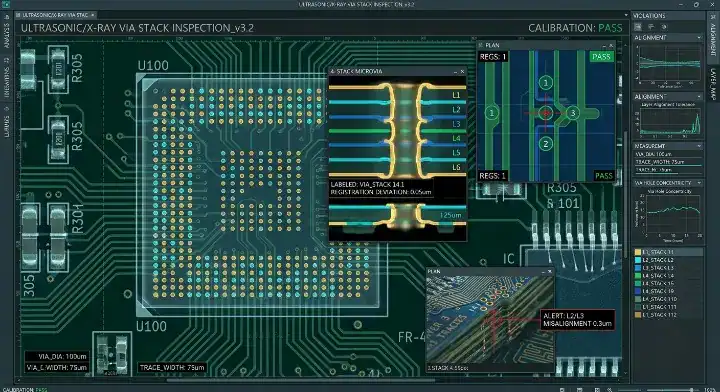
5. What Are the Yield Differences Between ELIC and Sequential Lamination?
The yield gap between these two build types is massive. If your design is targeted for harsh environments, you must reference IPC-6016 Qualification and Performance Specification for High Density Interconnect (HDI) Layers or Boards to understand how thermal cycling affects reliability.
On the EEVBlog and All About Circuits forums, engineers often ask: “What yield should I realistically expect from ELIC vs 2+N+2 builds at the same layer count?”
“We’ve tracked yield across approximately 240 HDI build types over 24 months. A 2+N+2 build with our standard process averages 94.5% first-pass yield. A 3+N+3 build drops to roughly 88% — the extra lamination cycle is the killer because each thermal cycle compounds dimensional change and increases registration risk. Full any-layer ELIC on a 12-layer build runs about 82% first-pass yield, our absolute floor among production processes. The yield gap is not in the drilling or plating — those processes are stable. The gap is in registration: every additional lamination cycle adds dimensional mismatch between layers, and ELIC requires perfect microvia-to-pad alignment on every layer pair. We charge ELIC at roughly 2.2× the price of 2+N+2 for the same layer count, and 30% of that premium is yield insurance built into the per-panel cost. For customers who can route their design in 2+N+2 without forcing the issue, we save them money by talking them out of ELIC.”
The Core Root of Yield Loss: Layer Registration
Every time a panel is pressed in a lamination cycle, the glass-reinforced epoxy expands and contracts. Each lamination cycle introduces an inescapable dimensional registration offset of 12 to 18 microns per layer.
By the time you reach 11 lamination cycles in a 12-layer ELIC board, the cumulative registration skew is highly volatile. If your layout features aggressive microvia capture pads, a 15 microns registration drift will result in the laser drill missing the target pad, leading to an open circuit.
To improve ELIC yields by 5% to 8%, designers must relax their microvia capture pad diameter (annular ring) to 50 microns or more wherever layout space permits.
6. How Does Lamination Cycle Count Affect HDI Cost and Reliability?
The reliable life of an HDI board is directly inversely proportional to its lamination cycles. Every pass through a lamination press subjects the copper foils, internal glass fibers, and cured resins to extreme thermal expansion stress along the Z-axis.
In sequential lamination, having a solid inner core limits the volumetric expansion of the overall stack. However, in an ELIC board, the absence of a thick, stabilizing core combined with continuous columns of stacked microvias introduces significant Coefficient of Thermal Expansion (CTE) mismatch risks.
During assembly reflow (which reaches peaks of 260 degrees Celsius for lead-free solder), the resin expands much faster than the solid copper columns. This Z-axis expansion places immense tensile stress on the microvia joints. If the lamination chemistry or plating was not flawless, this stress will pull the microvia base away from its target pad, creating an intermittent or permanent open circuit.
7. What Materials Work Best for ELIC vs Sequential Lamination?
Choosing the right materials is critical to surviving the sequential lamination gauntlet. Because ELIC undergoes so many thermal cycles, you cannot use standard FR-4 prepregs.
Table 2: Material Requirements for ELIC vs Sequential Lamination
| Material Attribute | Sequential Lamination (e.g., 2+N+2) | Any-Layer ELIC |
|---|---|---|
| Prepreg Type | Standard No-Flow or Low-Flow Prepreg | Resin-Coated Copper (RCC) or Ultra-Low Flow High-Tg Prepreg |
| Glass Transition Temp (Tg) | 150 to 170 degrees Celsius | 180 degrees Celsius or more (High-Tg, low-expansion material mandatory) |
| Z-Axis CTE (Pre-Tg / Post-Tg) | 45 ppm/°C / 230 ppm/°C | 30 ppm/°C or less / 180 ppm/°C or less |
| Copper Foil Type | HTE (High-Temperature Elongation) Foil | VLP (Very Low Profile) or Ultra-VLP Foil (for sub-30 micron traces) |
Any-layer ELIC demands ultra-low CTE materials (like Panasonic Megtron 6 or Isola I-Speed) to prevent the laminate from ripping apart the copper-filled stacked vias during successive lamination presses.
8. How Do Microvia Stack Requirements Differ Between Build Types?
To safely route microvias without risking field failures, designers must understand physical aspect ratio limitations. The foundational layout guidelines for these vias can be found in IPC-2315 Design Guide for High Density Interconnects (HDI) and Microvias.
The routing capacity and physical Z-axis stack behavior differ dramatically between sequential and any-layer builds:
- Sequential Stackups: Rely on staggered or strictly limited stacked microvias. Staggering microvias (e.g., Layer 1-2 blind via offset from Layer 2-3 blind via) is highly reliable but consumes lateral layout routing channels. To maintain high reliability, designers should calculate the optimal HDI microvia aspect ratio sweet spot (ideally targeting an aspect ratio of 0.8:1 or less).
- ELIC Stackups: Rely entirely on continuous stacked microvias. Staggering is technically possible but defeats the purpose of choosing an any-layer board. The Z-axis stack must be a solid, contiguous pillar of electroplated copper. Because there is no core, the registration of these microvias must be controlled via highly specialized DFM layout rules.
9. What Applications Truly Require ELIC vs Traditional HDI?
For many commercial consumer electronics, standard sequential lamination is the target choice because of its balanced price and high yields. But for ultra-high-density systems, ELIC is the only viable path.
Table 3: HDI Build Type Decision Matrix by Application
| Application / Hardware | Ideal BGA Pitch | Min Trace/Space | Recommended Build Type | Cost vs. Density Assessment |
|---|---|---|---|---|
| Consumer Wearables | 0.5mm or more | 50 microns / 50 microns | 1+N+1 or 2+N+2 | Highly cost-effective; sequential builds provide plenty of room. |
| Flagship Smartphones | 0.35mm – 0.4mm | 30 microns / 30 microns | Any-Layer ELIC (10-14 Layer) | Mandatory; extreme component density dictates Z-axis microvia stacking. |
| AI/GPU Accelerator Cards | 0.6mm (high pin count) | 40 microns / 40 microns | Any-Layer ELIC or 4+N+4 | High signal integrity and thermal stability require solid copper pillars. |
| Infotainment & ADAS | 0.5mm or more | 60 microns / 60 microns | 2+N+2 Sequential | Automotive reliability favors fewer lamination cycles to prevent CTE fatigue. |
| Industrial / Medical Implants | 0.4mm or less | 40 microns / 40 microns | Any-Layer ELIC (thin coreless) | Necessary for extreme space constraints and low loop-inductance. |
“An AI accelerator startup approached us in Q3 with a custom inference card design targeting hyperscale deployment. The board housed a 4,096-ball BGA at 0.6mm pitch alongside 128GB of HBM3 stacks — physically impossible to escape-route in conventional 2+N+2 HDI. We modeled four build options for them: 2+N+2 with daughter card breakouts ($340/board, mechanically unacceptable), 3+N+3 with aggressive trace narrowing ($580/board, signal integrity marginal), full ELIC 14-layer ($720/board, clean SI), and ELIC 16-layer ($890/board, future-proofed). They chose 14-layer ELIC. Total tooling and qualification took 14 weeks including thermal cycle testing per JESD22-A104 and HALT validation. Yield on their first 500-unit pre-production run hit 79% — five points under our average for ELIC, attributable to their unusually aggressive trace impedance tolerances. By the second 2,000-unit run our yield was 86% with the calibrated process. Per-unit cost at 50K annual volume settled at $640 — higher than they’d hoped, but the only achievable path to their hardware.”
10. How Do You Specify HDI Build Type in Your Fabrication Notes?
When handing over Gerber or ODB++ files to an HDI PCB manufacturer, clarity in your fabrication drawing prevents expensive tooling hold-ups. Do not simply label a drawing as “ELIC” or “Sequential” without explicit stackup rules.
To specify your build types correctly, your fab notes must contain:
- A Precise Stackup Diagram showing exactly which dielectric layers correspond to which laser drill cycles (e.g., L1-L2, L2-L3, L3-L4 drill layers).
- Clear Drilling Definitions: For ELIC, explicitly state: “All blind microvias must be solid copper-plated to flat profile (maximum dimple of 5 microns or less) to support continuous vertical stacking.”
- Detailed Lamination Instructions: Specify the maximum allowed cumulative lamination cycles and target Tg/CTE material classifications (e.g., Isola I-Speed or equivalent).
- Registration Tolerances: Outline the minimum acceptable annular ring for laser drill target pads (recommend targeting 50 microns or more for ELIC yields).
If you are looking to optimize your production budget, consider reading our guide on sequential lamination cost reduction to save up to 30% on complex build configurations.
Frequently Asked Questions (FAQ)
What is the cost difference between ELIC and 2+N+2 HDI?
For the same layer count, ELIC costs approximately 2.2x a comparable 2+N+2 sequential lamination build. The cost breakdown: copper-fill electroplating adds about 25%, multiple lamination cycles add about 30%, microvia drilling adds about 15%, and yield buffer adds about 20%. For a 12-layer board at moderate volume, expect ELIC pricing of 400 to 700 dollars per panel versus 180 to 320 dollars for 2+N+2.
Which applications truly require any-layer ELIC?
ELIC is required when: BGA pitch is 0.4mm or less with more than 1500 I/O, high-speed differential pairs exceed 8 to 12 in a constrained area, or layer count must stay 14 or less while supporting dense escape routing. Typical applications: flagship smartphones, AI accelerators (HBM-attached GPU/TPU cards), advanced 5G mmWave modules, and high-end SoC test boards. For BGA pitch of 0.5mm or more with less than 1000 I/O, 2+N+2 with smart routing usually works.
Can a standard HDI fabricator build ELIC?
No. True ELIC requires four pieces of dedicated capability: UV laser drilling for 50 micron vias, copper-fill electroplating with under 5 microns dimple control, precision vacuum lamination, and X-ray-based registration under 25 microns. Globally, fewer than 20 fabs can build production-volume ELIC reliably. Many fabs claim ELIC capability but actually offer only 1 to 2 layers of stacked microvia, which is not the same. Ask specifically about dedicated ELIC lines, recent yield data, and annual ELIC panel volume.
What’s the typical yield for ELIC versus sequential lamination?
Typical first-pass yields: 2+N+2 averages 94.5%, 3+N+3 drops to around 88%, and ELIC 12-layer averages 82%. ELIC 16-layer can fall to 75%. The yield gap is driven by registration mismatch — each additional lamination cycle adds 12 to 18 microns of layer-to-layer misalignment. Yield can be improved 5 to 8 percentage points by relaxing microvia annular ring to 50 microns or more at the design stage.
Upload your files today · Free DFM check before production · Ship worldwide
Get your PCB prototypes in as fast as 24 hours. We handle FR4, Rogers, and Flex up to 60 layers — free prototypes for 2–4 layer boards, no minimum order.
Just upload your Gerber + BOM — we source every part, assemble, and inspect (AOI + X‑Ray) so you don't have to chase suppliers. Boards ship in as fast as 24 hours.