
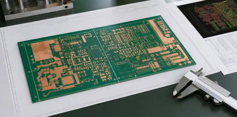
Quick Answer: PCB copper balance review should happen before CAM release when copper density, panel orientation, or process copper could change manufacturability. The buyer should freeze where copper may change, where design copper is controlled, and who approves supplier edits.
PCB copper balance is a manufacturing review of copper distribution across layers and panels before the supplier turns artwork into production CAM. Use this page when the released data looks electrically finished but the copper distribution may still create a CAM, plating, etching, or panel-balance question. The goal is to turn a vague supplier concern into a marked layer, a proposed action, and a named approval owner.
Table of Contents
- What should a buyer check first in copper balance?
- How does panel layout change the balance review?
- Which drawing notes prevent silent CAM changes?
- Where do warpage and copper balance overlap?
- What should CAM return before fabrication starts?
- How should procurement compare supplier answers?
- What belongs in the RFQ package?
- How can QueenEMS review a copper-balance hold?
What should a buyer check first in copper balance?
Start with the copper area map, not the finished board outline. A PCB can look symmetrical from the outside while one signal layer carries dense pours, another has large voids, and the panel edge carries very different plating exposure. The buyer’s first job is to identify where copper density changes could affect etching, plating, lamination pressure, or bow and twist.
Ask for a quick layer-by-layer review when the design has large plane cutouts, dense coil areas, heavy copper zones, large keepouts, RF clearances, or big copper differences between panel rows. This is narrower than copper thieving approval: the question here is whether the released artwork already creates a balance risk before any process copper is added.
CAM signal: if one layer has a large empty region beside dense copper, require a CAM note that identifies whether the supplier may add nonfunctional copper, adjust copper fill, or must hold the job for engineering approval.
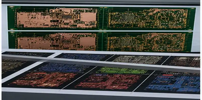
A practical review starts by exporting copper area by layer or at least marking the obvious dense and sparse zones. Buyers do not need to calculate exact copper percentage for every square millimeter, but they should know which regions are sensitive enough to stop CAM. That gives the supplier permission to solve routine process balance while protecting controlled electrical geometry.
A useful RFQ attachment is a marked PDF with three colors: copper-controlled areas, supplier-adjustable process areas, and no-copper keepouts. That simple map often works better than a long fabrication note because it shows CAM exactly where judgement is allowed.
For early capability screening, the buyer can send a simplified copper-density view instead of full product files when confidentiality is a concern. Production pricing still needs the real Gerber or ODB++ package because density risk can hide in small local regions.
How does panel layout change the balance review?
Panel layout can improve or worsen PCB copper balance because the supplier processes a panel, not an isolated CAD screenshot. A single board may be acceptable by itself but create uneven exposure when repeated in a mixed panel or rotated against another design.
Review the copper map at panel level when the order uses arrays, breakaway rails, mixed designs, or asymmetric tooling strips. The PCB panel drawing approval page owns the broader panel release decision; this article focuses only on how panel choices affect copper distribution and process stability.
| Copper-balance checkpoint | What to look for | Approval boundary |
|---|---|---|
| Sparse versus dense areas | Large voids beside heavy copper fields | Engineering approves copper additions in controlled zones |
| Panel rail influence | Copper-heavy rails or asymmetric tooling strips | Supplier marks rail changes before CAM freeze |
| Keepout conflict | Dummy copper near RF, antenna, HV, or cosmetic areas | No process copper without written approval |
Buyer call: do not approve the panel drawing until copper-heavy and copper-light regions have been checked against the supplier’s proposed orientation.
Panel balance also affects inspection and handling. A rail with heavy copper can stiffen one side of the panel, while a rail with little copper may flex differently during routing or depaneling. Asking about panel-level balance is especially useful when the board is long, thin, asymmetric, or paired with another design in a production panel.
For mixed panels, include the proposed array direction and any customer-required label orientation. Rotating a board can help copper balance, but it may create assembly handling or visual inspection problems if the panel direction is fixed elsewhere.
The supplier’s answer should also identify whether the issue is board-level or panel-level. Board-level problems usually require engineering review, while panel-level problems may be solved with orientation, rails, or process copper outside the shipped board.
Which drawing notes prevent silent CAM changes?
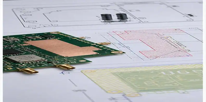
A useful drawing note tells the supplier what copper may change and what copper represents design intent. Without that boundary, a well-meant CAM correction can move clearances, alter local return paths, or add copper where the engineer intended an isolation region.
Write the note in operational language: ‘Nonfunctional copper for process balance requires approval inside RF, antenna, high-voltage, controlled impedance, cosmetic, or keepout areas.’ That sentence does not design the panel for the supplier; it tells CAM where a balance edit becomes an engineering change.
Signal: A supplier may still propose a change, but the quote response should name the affected layer and region instead of hiding the edit inside a generic DFM approval.
The drawing note should avoid designing the supplier’s CAM process. Its job is to define the buyer’s approval boundary. Strong notes name restricted zones and the approval owner; weak notes say only ‘no change without approval’ and then force the supplier to ask about every minor cleanup action.
Do not let copper balance wording override creepage, clearance, or RF isolation rules. When the same region has both manufacturing and electrical constraints, the electrical constraint should be listed first so the supplier knows why extra copper is restricted.
Keep the approval path short. One engineering owner should decide whether the proposed copper is electrically harmless, and one purchasing owner should decide whether the change affects the quoted delivery or cost.
Where do warpage and copper balance overlap?
Copper imbalance can contribute to bow and twist, but it should not become a duplicate warpage article. The overlap matters when copper weight, large copper planes, panel orientation, board thickness, and laminate symmetry combine into a mechanical risk.
Use PCB bow and twist acceptance for measurement method and acceptance limits. Use this copper-balance review to decide whether the released artwork or panel plan needs a hold before the board reaches that acceptance stage.
Release rule: if copper asymmetry is obvious and the board is thin, long, or panel-sensitive, ask for a copper-balance comment before treating bow/twist limits as enough protection.
Warpage questions are easier to solve when the buyer separates geometry from acceptance. Copper imbalance can be one root cause, but the acceptance limit still needs a measurement method and board condition. The copper-balance review decides whether the design is entering production with a preventable asymmetry.
When bow and twist are already a customer concern, ask whether copper balance changes are preventive or corrective. Preventive edits improve process margin before the lot is built; corrective edits after failed samples usually require a revised drawing or controlled deviation.
If a customer drawing forbids nonfunctional copper, do not override that rule casually. Ask whether the supplier can quote as released, quote with a deviation request, or suggest a controlled artwork revision.
What should CAM return before fabrication starts?
CAM should return a short, marked response when copper distribution raises a manufacturing question. The useful output is not a broad ‘DFM OK’ message; it is a list of layers, regions, proposed edits, and approval needs.
A clear response separates unchanged product copper from optional process copper. It should also say whether the edit affects impedance regions, high-voltage spacing, RF clearances, component land patterns, visible areas, or coupon representation. That distinction helps engineering approve quickly without rereading every Gerber layer.
| CAM response type | What it means for copper balance | Buyer decision |
|---|---|---|
| No balance edit needed | Supplier can build the released artwork | Keep Gerber and panel baseline locked |
| Add isolated process copper | Yield support is possible outside product geometry | Approve only after marked keepout review |
| Change panel orientation | Balance improves by rotating or rearranging boards | Confirm assembly, labeling, and breakaway effects |
Quote evidence: request one screenshot per questioned layer plus a written reason for each proposed copper-balance edit.
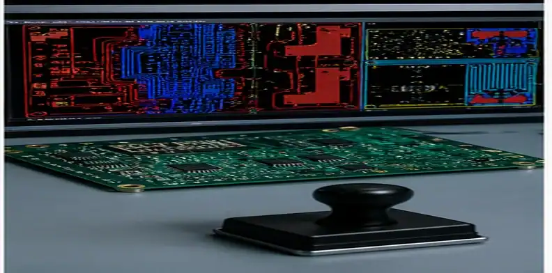
Marked CAM screenshots are more useful than long email descriptions. A screenshot can show whether the questioned copper sits under a component, near an RF feed, beside a high-voltage clearance, or only in a harmless tooling area. That makes approval faster and reduces the chance that purchasing approves a technical change without engineering context.
The CAM return should include layer names exactly as they appear in the data set. A note that says ‘outer layer issue’ is weaker than one that names L1, L2, panel rail, or solder-side copper because engineering can approve only what it can identify.
Copper-balance review is also useful for cosmetic boards. Added copper or density changes near visible areas may not affect electrical function but can still change appearance, solder mask behavior, or customer acceptance.
How should procurement compare supplier answers?
Procurement should compare copper-balance answers by assumptions, not only price. One supplier may quote with no CAM changes, another may assume process copper can be added, and a third may hold the job for engineering review.
Those are different manufacturing positions. A cheap quote that depends on unapproved dummy copper can become slower than a quote that names the hold immediately. Use the same discipline as a PCB DFM review before PO: compare what physical board the quote actually covers.
Buyer call: treat any unstated copper-balance assumption as a quote difference, not as a minor wording issue.
Supplier comparison should also consider timing. A quote that includes a one-day engineering hold may still be better than a fast quote built on an assumption. The buyer should compare the total route to a stable production file, not only the price cell in a spreadsheet.
When two suppliers answer differently, ask each one what happens if no copper-balance edit is approved. The answer exposes whether the job remains manufacturable, becomes lower-yield, requires a longer CAM cycle, or should be quoted as a design revision.
A good quote note says whether the balance review is closed, pending buyer approval, or included with a named assumption. That prevents the issue from resurfacing after the PO is issued.
What belongs in the RFQ package?
The RFQ package should include Gerber or ODB++, stackup, copper weights, panel preference, keepout notes, controlled geometry, cosmetic areas, and the approval owner for copper changes. If there are known sparse zones or copper-heavy regions, call them out directly instead of waiting for CAM to discover them.
For designs that also have stackup risk, include the supplier construction proposal and compare it with supplier stackup signoff. Copper balance and stackup are separate decisions, but they meet during lamination, finished thickness review, and warpage control.
RFQ signal: the better package tells the supplier where copper is process-adjustable and where it is controlled design geometry.
The package is stronger when it includes both product and panel intent. If panel format is flexible, say so. If assembly rails, break tabs, fiducials, or customer packing force a fixed panel format, say that as well so the supplier does not solve copper balance by changing something the assembly process needs.
For repeat orders, include the last accepted panel and copper-balance decision. A supplier may remember the process route, but the buyer should still keep the accepted CAM assumption tied to the revision being purchased.
If the design later changes copper pours, repeat the balance review. A revision that appears small on schematic may significantly change local copper area on one layer.
Revision control should also name the data source used for comparison. A screenshot from one CAM station, a panel PDF, and released ODB++ data can show the same copper issue differently, so the buyer should keep the accepted evidence format with the purchase record. That prevents the next supplier review from reopening a settled decision just because the visual reference changed.
How can QueenEMS review a copper-balance hold?
Use this review when a CAM question asks to add, remove, or rebalance copper and the buyer is not sure whether the change is only process copper. The useful package is small: released Gerber or ODB++, proposed panel view, stackup, copper weights, the marked CAM concern, and the supplier’s requested edit.
Acceptance rule: close the copper-balance question before CAM output becomes the production baseline.
For urgent orders, include the exact layer name, affected region, and any keepout, RF, creepage, cosmetic, or impedance note that limits copper addition. Send the marked hold package on the QueenEMS contact page so QueenEMS can return a copper-balance disposition: harmless CAM cleanup, engineering approval item, panel-layout concern, or PO-release hold.
FAQ
Is PCB copper balance the same as copper thieving?
No. Copper balance is the distribution condition being reviewed, while copper thieving is one possible process method for improving that condition.
Can CAM add copper without engineering approval?
Only when the RFQ allows it and the added copper stays outside controlled electrical, RF, high-voltage, cosmetic, and keepout regions.
Does copper balance always create bow and twist?
No. It is one contributor. Board thickness, laminate symmetry, copper weight, panel design, and assembly heat also affect bow and twist.
Written by the QueenEMS Engineering Team
Upload your files today · Free DFM check before production · Ship worldwide
Get your PCB prototypes in as fast as 24 hours. We handle FR4, Rogers, and hybrid boards up to 40 layers in volume production, with advanced builds subject to engineering review — free prototypes for 2–4 layer FR-4 boards, no minimum order.
Just upload your Gerber + BOM — we source every part, assemble, and inspect (AOI + X‑Ray) so you don't have to chase suppliers. Boards ship in as fast as 24 hours.