
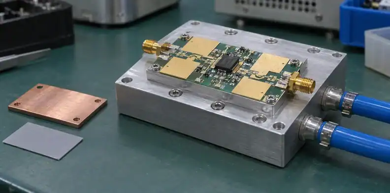
Quick Answer: GaN amplifier PCB thermal design starts with the heat dissipated at the intended RF operating point and the package’s defined temperature reference. Continuous-wave operation requires a sustained path through the package, solder, board or copper coin, thermal interface and cold plate. Choose and validate that path together with the RF ground; a pulsed power result or a DC continuity check cannot establish full-power CW performance.
A GaN amplifier PCB thermal design that works during short RF pulses may need different cooling for continuous operation. The first decision is how much heat the actual device must shed, followed by whether the proposed package, board and cooling assembly can remove it while preserving the source return and matching network.
This is a real design question. A Qorvo forum discussion about continuous QPA2612 operation asks about pulsed datasheet conditions, copper coins and microwave grounding. The discussion identifies the problem; device-specific calculations still need the manufacturer’s data and the proposed assembly.
Table of Contents
- Define the CW operating envelope
- Calculate heat from the actual RF operating point
- Find the package heat path and temperature reference
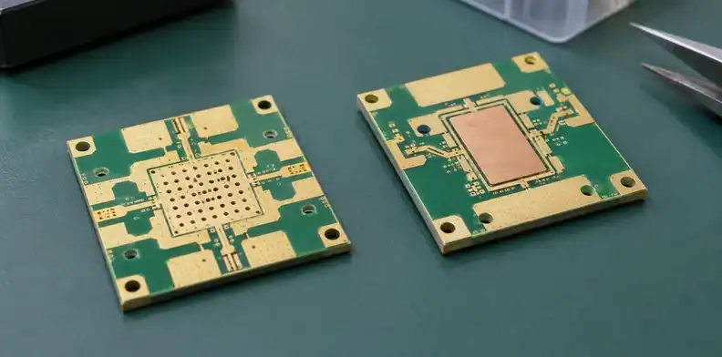
- Decide whether the RF board needs a copper coin
- Connect the coin as part of the RF ground
- Control the soldered pad and finished coin geometry
- Close the thermal path at the cold plate
- Measure temperature at the right reference point
- Prove CW thermal and RF behavior on the same prototype
- Release the RF thermal package for quotation
Define the CW operating envelope
GaN amplifier PCB thermal design requires the intended bias, RF waveform and cooling boundary before selecting the board’s heat-removal structure. Continuous wave, or CW, means the RF drive continues without the off-time used in a pulsed test. A modulated transmitter also needs its actual average power, peaks and duty behavior recorded; the word “continuous” alone does not describe its heat load.
Pulse width and duty cycle belong beside any thermal-resistance value taken from a datasheet. Qorvo’s channel-temperature application note explains how pulse conditions affect the temperature calculation. Multiplying on-state heat by duty cycle can estimate average heating under appropriate assumptions, but it does not describe the temperature reached within each pulse.
| Operating input | State it explicitly | Design consequence |
|---|---|---|
| RF drive | Frequency range, CW tone or modulation, input and output power | Defines the electrical operating point used for heat estimation |
| Bias | Supply voltage and driven current, including other supply rails | Separates operating dissipation from a quiescent-current assumption |
| Pulsing | Pulse width, repetition rate and duty cycle, if applicable | Determines whether transient thermal data are applicable |
| Cooling | Local cold-plate temperature, flow or airflow, and mounting arrangement | Defines the boundary against which the heat path is evaluated |
| Limits | Manufacturer temperature definition and agreed test stop criteria | Prevents a package-surface reading being used as a channel limit |
Consider a radar amplifier being adapted to a continuously driven test instrument. Its existing pulse measurements may still describe RF gain and matching, yet the sustained heating condition has changed. The new operating envelope should be issued as an engineering input before anyone quotes the same layout with an added coin.
Calculate heat from the actual RF operating point
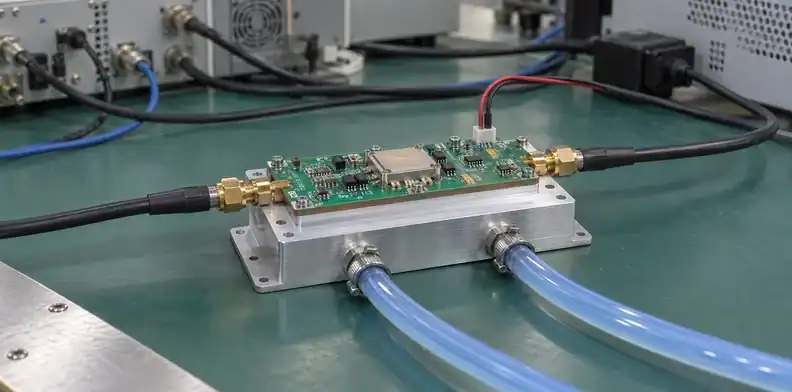
Calculate device heat from DC input and RF power at the same operating point. An amplifier described as “10 W” normally refers to RF output; that label does not establish a 10 W cooling requirement.
Calculate device dissipation with an energy balance
For an amplifier stage, the useful starting equation is Pheat = PDC + PRF,in − PRF,out. Qorvo’s PAE, dissipation and temperature calculator uses this energy balance. Keep the RF input and output measurement planes consistent, and account separately for regulator, driver, feed-line or passive-network losses outside those planes.
Take an illustrative operating point: 24 V at 1.0 A gives 24 W of DC input. With 0.1 W RF input and 10 W RF output, the estimated stage dissipation is 14.1 W. These are assumed values for explaining the calculation, rather than measurements of a particular GaN part or a QueenEMS board.
Drain efficiency uses RF output divided by DC input. Power-added efficiency, or PAE, subtracts RF input from RF output before dividing by DC input. If a datasheet provides efficiency instead of measured current, check which definition and drive condition it uses before reconstructing the heat load.
Check backed-off and modulated operating points
Repeat the calculation at the operating points the product actually uses. A backed-off amplifier may produce less RF output while retaining appreciable DC consumption; its heat cannot be scaled directly from the full-power output rating. Use driven current at that point, together with the corresponding RF input and output.
For modulation, average heat supports a steady thermal estimate, while time-varying power may require a transient model. Also check startup, bias-only dwell and frequency-dependent efficiency if they occur in normal service. The result should be a short operating-point sweep identifying which condition governs the prototype, rather than one optimistic heat figure.
Find the package heat path and temperature reference
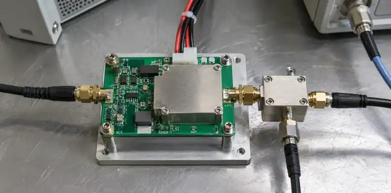
Use the manufacturer’s package drawing, layout guidance and thermal model to identify where heat leaves the device. A bottom-cooled exposed-pad package, a flange-mounted transistor and a deliberately top-cooled RF module place different demands on the PCB.
Dynax’s GaN HEMT thermal guide relates dissipation, case temperature and thermal resistance while distinguishing package and operating conditions. Its lesson for a board design is to preserve the stated reference point. A temperature measured on a distant chassis wall cannot be substituted for a case reference under the package without modeling the intervening path.
| Package arrangement | Trace this heat path | Confirm before board design |
|---|---|---|
| Bottom-cooled SMT package | Device → exposed pad → solder → board structure → cooler | Pad function, recommended land and the thermal-model reference |
| Flange-mounted device | Device → flange → mounting interface → heat spreader | Flange contact, fasteners and mounting instructions |
| Top-cooled RF module | Device → designated top contact → cooler | Approved top contact, mechanical loading and package guidance |
Top cooling is a real RF-package option: NXP documents it for a specific family of RF power modules. That architecture cannot be assumed for an ordinary bottom-cooled QFN, or quad flat no-lead package.
Check what the device thermal resistance already includes before adding board and interface resistances. The same reference temperature must join the device model to the assembly model. Keep the RF dielectric decision separate at this stage; the RO4000 laminate family discussion supports that material question without establishing a complete cooling solution.
Decide whether the RF board needs a copper coin
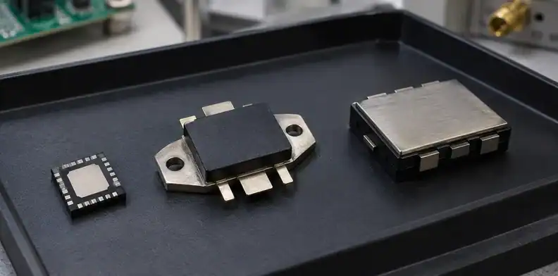
Choose a coin when the proposed via-based board cannot satisfy the device’s thermal requirements within the available thickness, footprint and cooling arrangement. The word “GaN” alone does not determine that choice. The actual package heat footprint and modeled path to the cooler do.
For a via solution, distinguish plated barrels, resin-filled capped holes and genuinely copper-filled structures. Their thermal behavior depends on the conducting cross-section, board thickness and interfaces. The copper-fill versus resin-fill process discussion helps identify which construction is being proposed; the thermal model still needs its actual geometry and materials.
A published thin RF board with copper-filled vias is useful evidence that a via path can be engineered for a particular assembly. It does not establish performance for a much thicker multilayer board. Changing thickness also changes the vertical heat route, so include the finished dimension and tolerance from the PCB thickness specification in the mechanical and thermal models.
For a coin candidate, assess the entire path from package pad to cold plate. A larger copper insert can spread heat, but its benefit depends on solder contact, backside contact and where the cooler receives that heat. Compare the candidates at the same dissipation and cooling boundary, then choose the one that can be fabricated, assembled and validated within the project constraints.
Connect the coin as part of the RF ground
Define the coin’s electrical net and its physical connections to the package return, board ground and cooling hardware. When the exposed package pad is the RF source return, the conductive path around the coin becomes part of the amplifier’s RF design.
Specify where the coin joins the source return
Start with the device’s recommended footprint and ground arrangement. Describe how the soldered pad connects to the coin face, how surrounding copper joins that face, and which plated or metallurgical connections join relevant ground layers. A schematic ground symbol leaves these dimensions unresolved.
Treat a cold-plate attachment as a separate connection unless its electrical role is explicitly designed. Surface coatings, thermal-interface materials, fastener locations and contact pressure can change its behavior. An electrically insulating TIM can carry heat while leaving the intended RF return entirely dependent on the PCB’s connections.
DC resistance testing can establish that a connection exists. Microwave return behavior also depends on its geometry and distributed impedance. A thin, remote ground connection may pass continuity while failing to reproduce the return path used in the manufacturer’s evaluation layout.
Include the connection in the electromagnetic model
Include the coin boundary, ground contacts, nearby transmission lines and relevant carrier geometry in the electromagnetic model. Check whether the insert changes source inductance, current distribution, matching or coupling. Keep the package reference planes consistent with the device model.
These checks extend beyond a trace-width calculation. The controlled-impedance specification should still define the RF line and reference plane, while the coin connection needs its own geometry and verification. Agree with the RF designer which fabrication changes require a new simulation or prototype measurement before releasing an altered ground arrangement.
Control the soldered pad and finished coin geometry
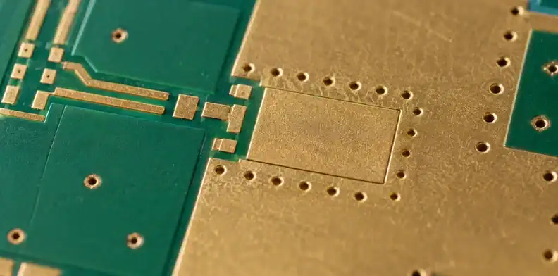
Specify coin height and flatness relative to the assembled package lands, then check the resulting thermal-pad solder joint. The package must form its intended lead joints and thermal connection in the same assembly operation; examining the bare coin alone cannot establish that fit.
| Interface issue | Potential effect on the RF assembly | Evidence to review |
|---|---|---|
| Coin face proud of adjacent lands | Alters the package seating and lead-joint geometry | Finished surface measurements tied to the package land drawing |
| Coin face recessed | Increases the pad-to-coin gap or leaves incomplete contact | Cross-section or assembly study of the proposed stack |
| Incomplete solder coverage | Interrupts the intended heat and electrical path locally | Joint inspection correlated with prototype behavior |
| Finish or paste substitution | Changes wetting and assembly assumptions | Approved finish, paste and process revision |
| Backside height variation | Changes cold-plate contact even with an acceptable top joint | Backside measurements and assembled interface checks |
Use the QFN assembly discussion for the broader footprint and assembly context. For this amplifier, the added question is whether the package pad, coin and surrounding lands form the thermal and RF geometry that was modeled.
X-ray inspection of hidden solder joints can reveal joint coverage and void locations beneath an exposed pad. It does not directly measure thermal resistance or channel temperature. Agree on acceptance using the package guidance and validation needs, including void location and contact continuity, rather than importing one universal percentage from an unrelated assembly.
Detailed bare-board fit and inspection belong in the embedded copper coin acceptance specification. Carry the approved finished geometry into the assembly drawing so a compliant bare board and a compliant solder process describe the same interface.
Close the thermal path at the cold plate
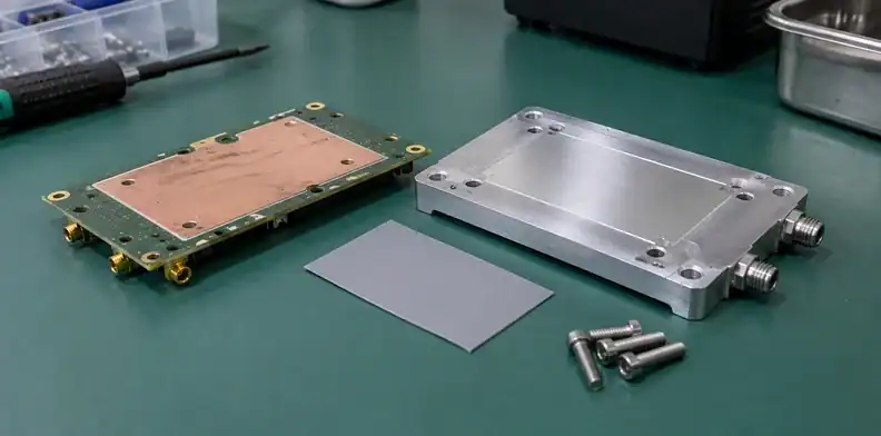
Specify the assembled backside contact, TIM and mechanical loading. A thermally conductive coin needs a controlled destination for its heat; the cold plate’s temperature and the resistance of the contact between them remain part of the design.
Define the assembled cold-plate boundary
Record the cold-plate contact area, local temperature reference, surface condition and fastener arrangement. Identify any recess, insulating layer or stand-off that interrupts the assumed coin-to-plate path. The board’s top-side geometry can look correct while its backside still leaves an uncontrolled gap.
Qorvo’s thermal-analysis application note discusses interface and measurement conditions in RF assemblies. Its package-specific recommendations need to be read with their mounting context. A flange interface thickness is not automatically the correct bond line for a small QFN coin.
Choose a TIM using the achievable bond-line thickness, electrical isolation requirements, contact pressure and service conditions. Define the assembly procedure as well as the material. Screw torque alone does not establish local contact pressure or confirm that a board has seated against the intended surface.
Estimate what a small interface gap can cost
An illustrative one-dimensional calculation shows why the gap matters. Assume a uniform 50 µm TIM layer, conductivity of 5 W/m·K and effective contact area of 25 mm². Using R = thickness / (conductivity × area) gives 0.4 K/W; the illustrative 14.1 W heat load would produce about 5.6°C across that ideal layer.
Doubling the assumed thickness to 100 µm doubles that resistance and temperature difference. This calculation excludes spreading, surface-contact resistance and nonuniform heat flow, so it is not a complete assembly prediction. Measure the actual bond line under the proposed clamp and board geometry to check this assumption.
For a serviceable assembly, repeat the mounting operation during prototype work. Comparing local temperatures after controlled reassembly can reveal sensitivity to the mechanical interface before a production drawing freezes it.
Measure temperature at the right reference point
Record where and how each temperature is measured, then state what that observation can establish. Package surface, coin backside, cold plate and transistor channel are different locations. A useful report keeps measured temperatures separate from calculated channel temperature.
| Observation | What it helps establish | Limit on interpretation |
|---|---|---|
| Thermocouple at an agreed local reference | Temperature history at that physical point | Position and mounting can differ from the datasheet case reference |
| Infrared view of the package or board | Surface-temperature distribution and visible hot regions | Emissivity, spatial resolution and hidden heat sources affect the reading |
| Local cold-plate sensor | Cooling boundary near the assembly | Does not include the coin, solder or package temperature rises |
| Driven DC current and RF powers | Dissipation estimate during the thermal test | Needs consistent operating point and power measurement planes |
| Condition-matched thermal model | Estimated internal temperature and heat-path behavior | Depends on model definitions, contacts and correlation with measurements |
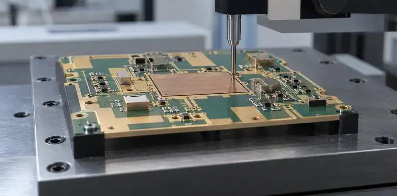
Plan sensor positions before building the test assembly. A thermocouple inserted into a contact region can disturb the interface it is supposed to observe. An accessible nearby sensor may be more practical, provided its offset from the required reference is addressed in the model and report.
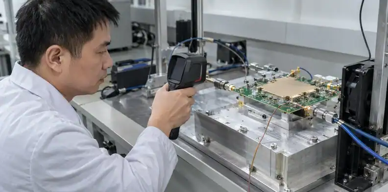
For infrared inspection, document the visible surface and the emissivity treatment or calibration used. A surface average cannot resolve an inaccessible channel hotspot merely because the camera produces a temperature map. The device’s own temperature definition must govern the comparison with its limit.
Use the temperature history to correlate the proposed heat path and locate unexpected gradients. If measured and predicted values diverge, investigate sensor placement, actual dissipation and contact assumptions before using the model to report channel temperature or reliability.
Prove CW thermal and RF behavior on the same prototype
Validate the intended RF operating point on the proposed cooling assembly through thermal equilibrium. Keep bias, drive, frequency, mechanical mounting and cooling conditions attached to each result, so a temperature trace and an RF power reading describe the same test.
Read the operating conditions behind a published design
Qorvo’s published 5 W X-band SMT amplifier design provides a useful external engineering example. It uses an 8 mil RO4003 board with copper-filled through vias and an aluminum carrier. The report describes CW small-signal measurements, while its large-signal power measurements use 500 µs pulses at 10% duty cycle.
The transfer problem is whether that published solution supports a new full-power CW assembly. The documented structure and measurements show what was built and under which conditions it was tested. They do not establish the sustained full-power temperature of a different device, thicker board or coin arrangement.
The engineering response is to preserve the manufacturer’s reference layout where applicable, model the proposed changes and test the intended continuous operating point. For a transfer to CW, document the new operating point and its measured result alongside the original pulse conditions. This keeps the proposed qualification traceable to the published example without assuming that its temperature behavior will carry over.
Test the proposed assembly through thermal equilibrium
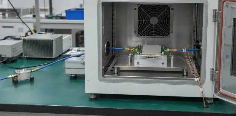
Begin with the approved bias and a controlled drive progression, using device-specific stop limits. Monitor current, RF input/output and local temperatures as the assembly warms. Check gain, matching and stability at the temperatures reached; an amplifier that stays electrically active may still drift outside the required RF performance.
Define equilibrium from an agreed temperature-rate criterion and test condition. Avoid substituting a fixed short run time without evidence that the assembly has settled. Record coolant or airflow conditions and any change in drive during the run.
If the design will use multiple frequencies, backed-off operation or modulation, exercise the conditions identified by the dissipation sweep. Preserve prototype photographs, sensor positions and mounting details with the results. Fabrication review through the RF PCB manufacturing service can address build feasibility; the RF designer must still approve circuit behavior and the device operating limits.
Release the RF thermal package for quotation
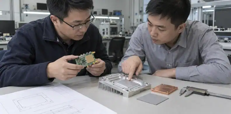
Send one consistent package covering the RF board, thermal interfaces and intended prototype verification. A quote based only on a copper-coin drawing leaves the operating heat, package joint and cooling hardware unresolved.
| Quotation input | Include | Decision it supports |
|---|---|---|
| Device and operation | Part/package, recommended footprint, frequency, driven current, RF powers and waveform | Identifies the heat source and operating conditions |
| RF board | Gerber or ODB++, stackup, finished thickness, controlled nets and approved material | Defines fabrication and electrical geometry |
| Coin and ground | Finished geometry, surface references, finish, net and layer connections | Makes the thermal insert and RF return explicit |
| Assembly and cooler | Pad/lead assembly requirements, cold-plate CAD, TIM and fastening arrangement | Establishes the complete physical heat path |
| Prototype scope | Quantities, sensor positions, thermal/RF tests and acceptance responsibilities | Separates the build quotation from qualification work |
Mark assumptions that remain open, especially the case-temperature reference, coin connection and cold-plate contact. A provisional feasibility quote can identify those open items, but production release should use their approved revisions. Include the same identifiers on the board drawing, mechanical assembly and test setup to prevent an apparently minor substitution from changing the heat path.
For a quotation, send QueenEMS the RF board and cooling-assembly package, including the device part number, CW dissipation estimate, coin-ground geometry and cold-plate interface. State whether the request covers bare-board fabrication, assembly or agreed prototype checks so the quoted scope matches the engineering decision.
Sources
- Qorvo: Understanding Thermal Analysis of RF Devices.
- Dynax: Thermal Performance Guide for GaN HEMT Transistors.
Written by the QueenEMS Engineering Team
Upload your files today · Free DFM check before production · Ship worldwide
Get your PCB prototypes in as fast as 24 hours. We handle FR4, Rogers, and hybrid boards up to 40 layers in volume production, with advanced builds subject to engineering review — free prototypes for 2–4 layer FR-4 boards, no minimum order.
Just upload your Gerber + BOM — we source every part, assemble, and inspect (AOI + X‑Ray) so you don't have to chase suppliers. Boards ship in as fast as 24 hours.