

Quick Answer: HDI stackup types follow IPC-2226 classification (Type I to VI) and i+N+i notation to define microvia layers. Choose 1+N+1 for 0.65-0.8mm BGA pitch (cost baseline, 1× lead time). Choose 2+N+2 for 0.4-0.5mm pitch (1.5-2× cost, supports 40% more routing channels). Choose ELIC for ≤0.35mm pitch (4-8× cost, 7-10 lamination cycles). The decision must be made before layout begins—switching later forces a complete redesign.
Key takeaways:
- Cost Baseline: 1+N+1 architecture uses a single layer of microvias and represents your lowest cost entry into HDI.
- Fine-Pitch Support: 2+N+2 structures handle 0.4mm BGAs perfectly but extend lead times to 18-25 days.
- Yield Risks: ELIC (Any-Layer) costs up to 8 times more because compounding lamination cycles create severe cumulative yield risks.
- Design Rule: A laser-drilled microvia must never span more than one dielectric layer in a standard sequential buildup.
Table of Contents
- 1. What Are HDI Stackup Types and Why Does the Choice Matter Before Layout?
- 2. How Does the i+N+i Notation Map to IPC-2226 Type I Through Type VI?
- 3. When Should You Pick a 1+N+1 HDI Stackup Type?
- 4. How Do 2+N+2 HDI Stackup Types Handle Fine-Pitch BGAs?
- 5. What Makes ELIC (Any-Layer) HDI Different from Sequential Build-Up?
- 6. How Does BGA Pitch Drive Your Choice Between 1+N+1, 2+N+2, and ELIC?
- 7. What Cost and Yield Differences Should You Expect Across HDI Stackup Types?
- 8. Why Is Symmetrical Construction Mandatory for Every HDI Stackup?
- 9. How Do You Avoid Defining a Via Span Your Stackup Cannot Manufacture?
- 10. Which HDI Stackup Type Should You Specify for Your Application?
HDI stackup types determine your board’s physical architecture, routing density, and manufacturing cost based on microvia placement. You start routing a high-density board, only to realize halfway through that your 0.4mm BGA cannot escape on a standard multi-layer setup. Forcing microvias into a design late causes immediate DRC failures and ruins your budget. By evaluating your BGA pitch early and selecting the correct IPC-2226 buildup, you ensure smooth routing. Partnering with a facility that has proven HDI PCB manufacturing capabilities guarantees your chosen stackup is actually manufacturable.
1. What Are HDI Stackup Types and Why Does the Choice Matter Before Layout?
HDI stackup types dictate the exact sequence of laser-drilled microvias and lamination cycles, directly impacting your bare board cost by 1.5 to 8 times. Selecting the wrong type before layout forces a 100% redesign because via spans cannot simply be copied and pasted across different buildup categories.
Identifying the Breakout Layers
Every high-density component requires a specific number of escape routing channels. If you select a stackup with insufficient microvia layers, you will literally run out of physical space to connect your inner pins. Making this architectural decision before placing a single component aligns your CAD tool’s design rules with the factory’s actual pressing sequence.
The Cost of Late Changes
Because different buildups require entirely different materials and via geometries, changing your stackup midway through a project destroys all previous routing work. If you try to upgrade from a single-lamination board to a dual-lamination board later, you must delete and redraw thousands of traces.
Bottom line: Never start your layout until you mathematically prove that your chosen stackup provides enough routing channels for your densest component.
2. How Does the i+N+i Notation Map to IPC-2226 Type I Through Type VI?
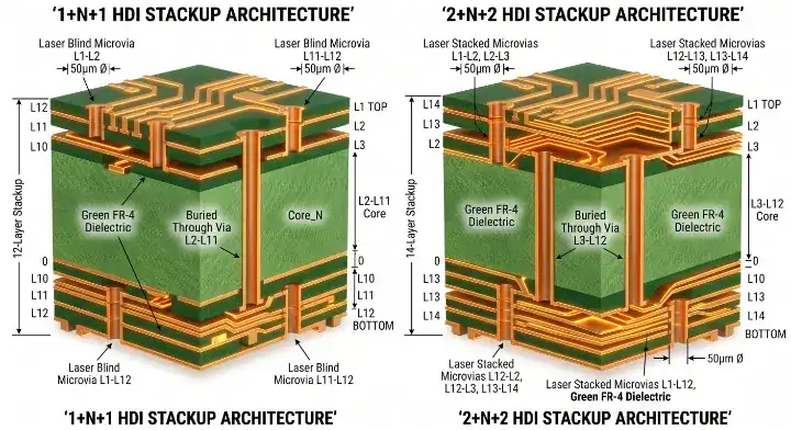
The i+N+i notation mathematically describes the buildup architecture, where “i” equals the number of sequential lamination cycles and “N” represents the standard core layers. This notation maps directly to IPC-2226 Type I through Type VI classifications to standardize manufacturing expectations globally.
Decoding the Variables
i+N+i notation is a structural naming convention where “i” dictates the outer laser-drilled microvia layers and “N” defines the buried core. Every “i” layer added increases fabrication cost by 15-25% due to extra pressing cycles. Understanding PCB stackup design fundamentals prevents costly specification errors during quoting.
IPC-2226 Classifications Explained
The IPC-2226 standard categorizes HDI into six formal types. Type I corresponds to a simple 1+N+1 without buried vias. Type II is a 1+N+1 that includes buried vias in the core. Type III represents a 2+N+2 structure utilizing stacked or staggered microvias. Types V and VI represent complex coreless Any-Layer structures.
| IPC-2226 Class | i+N+i Notation | Microvia Structure | Target Application |
|---|---|---|---|
| Type I | 1+N+1 | Outer to adjacent inner layer | Handheld GPS, simple routing |
| Type II | 1+N+1 | Outer layer + Core Buried Vias | Mid-range smartphones |
| Type III | 2+N+2 | Two buildup layers (stacked/staggered) | AI accelerators, DDR5 memory |
| Type V / VI | ELIC | Microvias on every layer | 5G phones, CPU packages |
Analysis Guide: Always match your required microvia depth to the correct IPC Type. Use Type I for baseline costs, and reserve Type III for dense memory routing.
Bottom line: Use standard IPC-2226 Type terminology alongside i+N+i notation in your fabrication notes to eliminate supplier confusion.
3. When Should You Pick a 1+N+1 HDI Stackup Type?
You should pick a 1+N+1 HDI stackup type when your tightest component is a 0.65-0.8mm BGA, keeping your manufacturing costs near baseline. This IPC-2226 Type I structure uses exactly one layer of microvias dropping to the adjacent inner layer, which perfectly handles moderate density without sequential lamination risks.
The Baseline Architecture
A 1+N+1 design is the most reliable entry point into high-density routing. Because it only requires one additional lamination press after the core is fabricated, the risk of layer misregistration remains incredibly low. This allows you to use standard FR4-Tg130 materials, saving significant money compared to high-Tg exotic resins.
The QueenEMS Engineering Perspective
Over-engineering a board wastes money and increases lead times unnecessarily.
- The Problem: A client submitted a massive 12-layer standard through-hole PCB scheme to route a moderately dense 0.65mm BGA, resulting in severe routing blocks and crosstalk.
- Our Solution: We transitioned the design to a highly optimized 1+N+1 8-layer HDI stackup.
- The Result: This change reduced the total board thickness by 38%, dropped bare board costs by 12%, and improved the first-pass yield to a flawless 94%.
Bottom line: For 0.65-0.8mm pitch BGAs with moderate pin counts, 1+N+1 delivers the absolute best cost-performance balance.
4. How Do 2+N+2 HDI Stackup Types Handle Fine-Pitch BGAs?
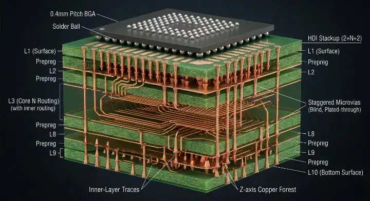
2+N+2 HDI stackup types handle fine-pitch BGAs by providing 40% more routing channels through two dedicated layers of laser-drilled microvias. This IPC-2226 Type III architecture easily supports 0.4-0.5mm BGAs but requires a 150°C+ high-Tg material to survive the multiple heating cycles.
Expanding Z-Axis Routing
A user on the FEDEVEL forum asked: “I’m using the MAX32666 with a 0.35mm pitch. We are trying to route it on a 6-layer standard board. Is there any alternative?” You cannot escape route a 0.35mm pitch on a standard 6-layer board because the through-holes block all internal paths. You must upgrade to a 2+N+2 8-layer setup using VIPPO (Via-in-Pad Plated Over). Utilizing 75µm laser microvias in a staggered configuration allows you to clear the inner pins without destroying your critical ground planes.
Stacked vs Staggered Reliability
In a 2+N+2 structure, you must choose between stacked or staggered microvias. Staggered microvias (offset by ≥100µm) are highly reliable because they distribute thermal expansion stress. If you choose stacked microvias to save space, you must require 100% void-free copper filling, verified by X-ray, to prevent the joints from cracking during reflow.
Bottom line: Upgrade to a 2+N+2 architecture only when your BGA pitch hits 0.4mm or 0.5mm with a pin count exceeding 500.
5. What Makes ELIC (Any-Layer) HDI Different from Sequential Build-Up?
ELIC (Every Layer Interconnect) eliminates the traditional drilled core entirely, using stacked copper-filled microvias across all 14-20 layers for absolute maximum density. This IPC-2226 Type V/VI approach supports extreme <0.35mm pitch components but introduces massive non-linear yield risks during production.
The Any-Layer Advantage
Traditional sequential build-ups rely on a stiff central core. ELIC builds up layer by layer from the center out, allowing signals to travel freely through any Z-axis path. This requires specialized low-Df (<0.005) spread-glass laminates. Applying advanced microvia design optimization prevents fracture risks across these deep stacks.
Identifying False ELIC Needs
Many designers believe they need ELIC when they simply have poor fanout strategies. If you can complete all escape routing in under 8 layers, you do not need ELIC. A well-designed 2+N+2 board with optimized sub-lamination can frequently replicate the density of an Any-Layer board at a fraction of the price.
Bottom line: ELIC is justified only when a 2+N+2 stackup combined with an aggressively optimized fanout strategy completely fails to complete the escape routing.
6. How Does BGA Pitch Drive Your Choice Between 1+N+1, 2+N+2, and ELIC?
BGA pitch directly drives your stackup choice: use 1+N+1 for 0.65mm, 2+N+2 for 0.4mm, and ELIC for ≤0.35mm to maintain high production yields. Misjudging this metric forces you into either unmanufacturable designs or massively overpriced bare boards.
The Pitch-to-Stackup Formula
A user on the SierraConnect forum asked: “How do I know if my design requires HDI or standard build-up?” HDI is strictly required when your BGA pitch hits 0.5mm or smaller. At ≥0.8mm, use standard boards. For 0.4-0.5mm, deploy a 2+N+2 architecture, and for ultra-dense <0.35mm processors, ELIC is your only functional option. Pin count also plays a role; a high pin count BGA (>500 pins) might require 2+N+2 even at a 0.65mm pitch simply because you need more escape channels.
| BGA Pitch | Recommended Stackup | Microvia Setup | Est. Cost Premium |
|---|---|---|---|
| ≥0.80mm | Standard Multi-layer | Through-hole | 1.0x (Baseline) |
| 0.65mm – 0.80mm | 1+N+1 HDI | Single layer microvia | 1.2x – 1.5x |
| 0.40mm – 0.50mm | 2+N+2 HDI | Staggered or Stacked | 1.5x – 2.5x |
| ≤0.35mm | ELIC (Any-Layer) | Fully Stacked Microvias | 4.0x – 8.0x |
Analysis Guide: Find your tightest BGA pitch on this chart to lock in your architecture before you route the first trace.
Bottom line: Your smallest BGA pitch strictly dictates your HDI buildup architecture; make this technical choice on day one of your project.
7. What Cost and Yield Differences Should You Expect Across HDI Stackup Types?
Upgrading from a 1+N+1 baseline to a 2+N+2 stackup doubles your cost and adds 18-25 days to lead time, while ELIC multiplies costs by 4 to 8 times. Because every lamination cycle adds a 15-25% price premium, you must perform a strict HDI vs standard PCB cost analysis before committing to advanced architectures.
Cumulative Yield Risks
A frustrated designer on EEVBlog asked: “We need very high density for our 0.3mm BGA. Considering ELIC. But the quote came back 8x our 2+N+2 quote. Is this normal?” Yes, this exponential jump is completely normal. ELIC requires 7-10 sequential lamination presses. If a defect occurs on the 9th press cycle, the previous 8 cycles of expensive materials and labor are instantly scrapped. This creates a massive cumulative yield risk, dropping average ELIC first-pass yields to 70-80% compared to 95% for 1+N+1 boards.
Delivery Schedules
More press cycles mean more days on the factory floor. A standard 1+N+1 board typically ships in 12-15 days. A 2+N+2 design extends that to 18-25 days. An ELIC board requires 30-45 days of intense manufacturing time, which severely impacts aggressive product launch schedules.
Bottom line: The 5-8× cost premium for ELIC reflects real cumulative yield failure risks, not arbitrary factory pricing.
8. Why Is Symmetrical Construction Mandatory for Every HDI Stackup?
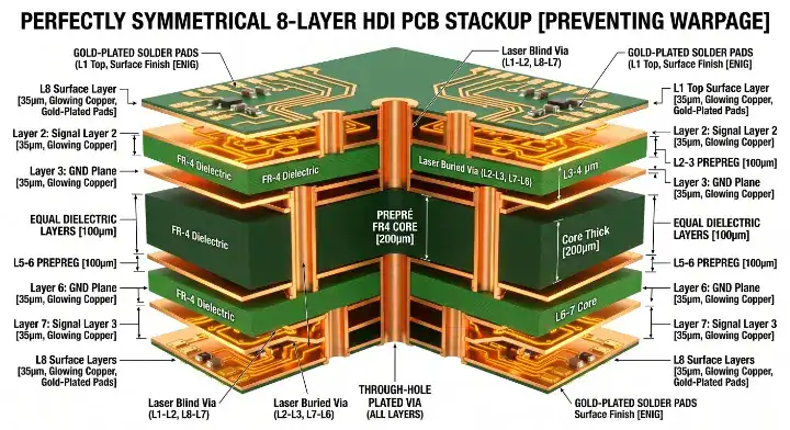
Symmetrical construction is mandatory because asymmetrical copper distribution causes severe bowing during lamination, pushing stackup warpage beyond the IPC-6016 0.75% limit. A warped 2+N+2 board will physically lift off the SMT stencil, resulting in a 100% assembly failure rate on fine-pitch BGAs.
The Dangers of CTE Mismatch
An engineer on SierraConnect noted: “My 2+N+2 stackup has 2oz copper on top and 1oz on bottom. Manufacturer flagged warpage risk. Why does symmetry matter so much for HDI?” Symmetry matters because HDI goes through high-heat lamination cycles repeatedly. CTE (Coefficient of Thermal Expansion) mismatch between uneven copper planes creates massive twisting forces during cooldown. You must use mirrored copper weights (±10%) and like-layer pairings (signal-to-signal, ground-to-ground) radiating out from the center core to keep the board flat.
Resin Flow Control
When pressing thin prepreg layers, the amount of copper on the adjacent layer dictates how the resin flows. If you have dense copper on Layer 2 and sparse copper on Layer 7, the dielectric thickness will compress unevenly, destroying your controlled impedance targets for high-speed signals.
Bottom line: Design your HDI stackup like a mirror; the top and bottom halves must have identical copper weights and dielectric thicknesses.
9. How Do You Avoid Defining a Via Span Your Stackup Cannot Manufacture?
You avoid defining an unmanufacturable via span by strictly limiting blind vias to span exactly one dielectric layer in sequential buildups. Specifying a microvia from Layer 1 to Layer 3 in a 1+N+1 architecture is physically impossible and causes 30% of all HDI no-bid rejections from factories.
Common Drill Definition Errors
Experts on the NextPCB blog emphasize: “The most frequent error is defining a via span that is physically impossible to manufacture in a single cycle.” A 1+N+1 stackup only permits laser microvias from L1 to L2. If your CAD tool places a microvia from L1 to L3, you are violating the 1:1 aspect ratio limit (per IPC-T-50M) and demanding a laser drill depth the factory cannot safely execute without burning through the board.
The QueenEMS Engineering Perspective
Ambiguous drill pairs halt production instantly.
- The Problem: A customer’s ODB++ files contained intersecting blind and buried via definitions that heavily mismatched their 2+N+2 stackup drawing.
- Our Solution: We implemented a strict Drill Pair definition checklist to map every start and stop layer to the correct lamination cycle.
- The Result: This verification eliminated all unmanufacturable spans and allowed us to release the board to production in just 4 hours instead of waiting 3 days for engineering queries.
Bottom line: Validate every single via span in your drill table against your stackup category before exporting your fabrication data.
10. Which HDI Stackup Type Should You Specify for Your Application?
You should specify 1+N+1 for industrial controllers, 2+N+2 for AI accelerators and DDR5 memory, and ELIC for ultra-compact 5G smartphones. Aligning your HDI stackup type with your exact application constraints guarantees you meet both electrical performance metrics and budget targets.
Evaluating the Six Dimensions
Choosing the right architecture requires balancing six critical dimensions in order of importance:
- Smallest BGA pitch: Dictates the minimum via geometry.
- Pin count: Drives the need for extra escape routing channels.
- Signal speed: Determines if via stubs must be completely eliminated.
- Form factor: Forces Z-axis compression.
- Volume target: Heavily influences the cost/yield trade-off.
- Fab capability: Ensures you do not design beyond reality.
Locking in the Decision
Do not guess your stackup. Measure your components, calculate your required channels, check your impedance needs, and lock in the simplest IPC-2226 Type that mathematically supports your layout.
Bottom line: Base your stackup specification entirely on mathematical routing channel requirements, never on layout guesswork.
Conclusion
Selecting between 1+N+1, 2+N+2, and ELIC is the single most consequential decision in high-density PCB design. If you choose an architecture that is too simple, your fine-pitch BGAs will fail to route; if you jump straight to ELIC, you will burn your budget on cumulative yield risks. By aligning your BGA pitch, pin count, and via spans with the correct IPC-2226 standards early on, you secure both your schedule and your wallet.
QueenEMS provides free front-end DFM reviews to help you validate your stackup architecture before you spend weeks routing. If you are struggling to escape route a 0.4mm BGA or want to optimize your buildup for cost, contact our HDI engineering team today. We will ensure your stackup is perfectly matched to your application’s density and budget.
Written by the QueenEMS Engineering Team
FAQs
Can I route a 0.35mm pitch BGA on a 1+N+1 stackup? No, a 0.35mm pitch BGA requires too many fine escape channels and cannot physically fan out using just one microvia layer. You must use at least a 2+N+2 stackup or an ELIC architecture to clear the dense inner pins successfully.
What is the main cost difference between 1+N+1 and 2+N+2? The main cost difference is the extra sequential lamination cycle required for 2+N+2. Pressing the board a second time adds 15-25% to the base cost, increases laser drilling time, and extends the overall manufacturing lead time by nearly a week.
How do I know if I need staggered or stacked microvias? Staggered microvias are the preferred, reliable choice for standard HDI. You only need stacked microvias when physical board space is so incredibly restricted that you cannot afford the 100µm offset required for staggering. Stacked vias require expensive 100% void-free filling.
What does the “N” mean in HDI stackup types? The “N” in i+N+i notation represents the standard, mechanically drilled inner core layers of the PCB. For example, in a 2+4+2 stackup, the “4” means there are four standard inner layers buried beneath two layers of laser-drilled microvias on each side.
Is ELIC always better for high-speed signal integrity? Yes, ELIC offers excellent signal integrity because it completely eliminates via stubs and allows extremely short, direct signal paths. However, the massive 5-8x cost premium means you should only use it if standard 2+N+2 structures cannot meet your specific impedance or density goals.
Upload your files today · Free DFM check before production · Ship worldwide
Get your PCB prototypes in as fast as 24 hours. We handle FR4, Rogers, and Flex up to 60 layers — free prototypes for 2–4 layer boards, no minimum order.
Just upload your Gerber + BOM — we source every part, assemble, and inspect (AOI + X‑Ray) so you don't have to chase suppliers. Boards ship in as fast as 24 hours.