
Quick Answer: Optimizing pcb panelization for assembly can increase SMT throughput by 300% and reduce unit costs by 15% to 25%. For mass production, a panel size between 150mm and 250mm wide is the “sweet spot” that minimizes PCB warping while maximizing machine rail utilization. Using V-score for straight edges saves 10% in area, but requires a 3.0mm component keep-out zone to prevent solder joint cracking during depaneling.
Key takeaways:
- Choose V-score for rectangular boards to save material; use Tab-route for irregular shapes.
- Maintain a 3mm to 5mm keep-out zone from the depaneling line for all SMT components.
- Add global fiducials to panel corners to achieve ±0.05mm placement accuracy.
- Limit panel width to 460mm to fit standard SMT conveyor rails.
Table of Contents
- Why Does Panel Design Matter for PCB Assembly Quality?
- V-Score vs Tab-Route vs Laser Depaneling: Which Method Fits Your Board?
- How Does Panel Layout Affect SMT Pick-and-Place Efficiency?
- What Panel Design Mistakes Cause Assembly Defects?
- How Many Boards Per Panel Is Optimal for Cost and Yield?
- What Are the Tooling Strip and Fiducial Requirements for SMT Panels?
- How Does Depaneling Stress Affect Component and Solder Joint Reliability?
- Panel Design Checklist: What to Verify Before Sending Files to Your CM
Your choice of panel layout is the single biggest factor in determining your final SMT production efficiency. While you may have already read about how to reduce PCB panel costs from a fabrication perspective, the assembly phase introduces entirely different mechanical and thermal stresses. QueenEMS maintains a 99.7% first pass yield benchmark because we vet every panel design for SMT-specific risks before the first stencil is cut. If you ignore how your panel interacts with the pick-and-place rails or reflow heat, you risk board warping, component cracking, and expensive manual rework.
Why Does Panel Design Matter for PCB Assembly Quality?
Proper pcb panelization for assembly creates a rigid, standardized frame that allows SMT machines to process dozens of boards in a single pass with ±0.05mm placement accuracy. A well-designed panel minimizes mechanical flexing during high-speed component mounting and prevents thermal warping inside the 250°C reflow oven, which directly protects delicate BGA solder joints from fracturing.
Here is the reality: The SMT machine doesn’t see your individual board; it sees the panel. If the panel is too flimsy, the board will “bounce” under the pressure of the placement head, leading to misaligned parts. If the panel is too heavy, it creates thermal sinks that cause uneven soldering.
Panelization in assembly serves three critical functions:
- Throughput Multiplication: Placing 10 boards in a panel reduces load/unload time by 90%.
- Mechanical Stability: Tooling strips provide the necessary “edge” for conveyor belts to grip the board without touching components.
- Global Alignment: Panel-level fiducials allow the machine to correct for board-to-board variations across the entire array.
Building a production-ready assembly panel layout is about balancing material savings with mechanical rigidity.
Bottom line: A panel design that prioritizes assembly rigidity over raw material savings will always result in a lower total cost per good board by reducing scrap and rework.
V-Score vs Tab-Route vs Laser Depaneling: Which Method Fits Your Board?
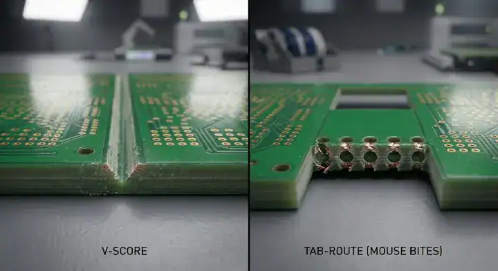
Choose V-score depaneling for rectangular boards to achieve zero-gap spacing and save 10-15% on material costs, but switch to tab-routing (mouse bites) for boards with irregular shapes or overhanging components. V-score is a mechanical cut that leaves a 0.3mm to 0.5mm residual web, while tab-routing uses small perforated bridges to hold boards in place, offering much lower stress during final separation.
| Method | Mechanical Stress | Board Edge Quality | Tooling Cost | Best For |
|---|---|---|---|---|
| V-Score | Moderate (Shear) | Rough (Straight) | Low | Standard rectangular boards |
| Tab-Route | Low (Vibration) | Smooth (with bites) | Moderate | Irregular shapes, circles |
| Laser Cut | Zero | High (Burr-free) | High | Ultra-thin or high-flex PCBs |
| Combo | Mixed | Varied | Moderate | Complex arrays with internal cutouts |
Comparison Anchor: Choose V-score if your board has straight edges and components are 3mm+ away from the line. Choose Tab-route if you have rounded corners or need to mount connectors that hang off the PCB edge.
Bottom line: Never use V-score for boards thinner than 0.8mm; the mechanical stress of “snapping” the boards apart will likely crack nearby MLCC capacitors.
How Does Panel Layout Affect SMT Pick-and-Place Efficiency?
An optimal pcb panelization for assembly layout reduces the “travel distance” of the placement head, potentially shaving 5 to 15 seconds off the cycle time for every panel processed. By orienting all boards in the same direction, you allow the SMT machine to use “gang-picking” for identical components, which significantly increases the units-per-hour (UPH) rating of the production line.
When you design an assembly panel layout, consider the machine’s dual-delivery system. If you mirror or rotate boards in the panel (e.g., 180-degree rotation), the machine must often stop to recalibrate the component orientation for every second board, which kills throughput.
- Uniform Orientation: Always keep the “Pin 1” of all ICs facing the same direction across the panel.
- Standard Rail Width: Design your panel width to be between 100mm and 250mm for the best stability on the conveyor.
- Symmetry: A symmetrical layout prevents the panel from bowing during the reflow process.
Bottom line: Keep all boards oriented in the same direction within the panel to maximize SMT machine UPH; 180-degree rotations should only be used as a last resort for material nesting.
What Panel Design Mistakes Cause Assembly Defects?
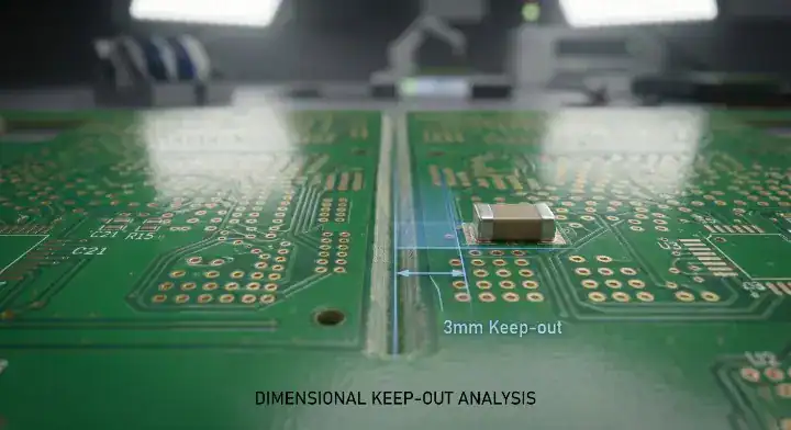
The most common panel design mistake is placing MLCC capacitors (like 0402 or 0603 packages) within 3.0mm of a V-score line, which leads to a 3-5% scrap rate due to micro-cracking during depaneling. Another frequent error is forgetting to add panel-level fiducials, which forces the SMT machine to rely on board-level marks that may have drifted during the PCB fabrication process.
| Parameter | Recommended Value | Consequence if Violated |
|---|---|---|
| SMT Keep-out | >3.0mm from V-score | Ceramic capacitor cracking (MLCC failure) |
| THT Keep-out | >5.0mm from V-score | Solder joint fracturing or pin bending |
| Fiducial Count | 3 per panel corners | Global alignment failure, ±0.2mm offset |
| Tooling Strip | 5.0mm to 7.0mm width | Conveyor rails will crush edge components |
Definition + Data: Global Fiducials are 1.0mm to 1.5mm copper circles placed on the panel corners that provide a universal coordinate system for SMT machines. Without at least 3 global fiducials, placement accuracy drops by nearly 50%.
Factory Perspective (EEAT): We see pcb panel design smt mistakes on roughly 1 in 5 new customer projects. The most expensive one last quarter involved a wearable device client who designed a 4-up panel with V-score separation but placed a row of 0201 capacitors 0.8mm from the line. During depaneling, the snap stress cracked 6 out of 200 boards—a 3% scrap rate on a $22/board assembly. We caught it on the first panel and stopped production, but the client had to move components 3mm away and re-make the stencil. This caused an 8-day delay and $1,200 in avoidable costs. Now, we flag any component within 3mm of a V-score during our DFM design for manufacturing review.
Bottom line: Follow the 3mm keep-out rule for all SMT parts near any depaneling line to avoid high-cost field failures caused by invisible capacitor cracks.
How Many Boards Per Panel Is Optimal for Cost and Yield?
The optimal number of boards per panel is determined by the “460mm rail limit” of standard SMT machines and the 150mm “warping threshold” of the reflow oven. While putting 50 boards on a massive 400mm x 400mm panel seems cheaper, the panel will likely sag in the center during reflow, causing a 10% increase in soldering defects like “tombstoning” or “bridging.”
According to IPC standards, the larger the panel, the more it will flex. For boards thinner than 1.6mm, we recommend keeping the panel width under 200mm unless you are willing to invest in custom carrier pallets.
| Board Size | Optimal Panel Layout | Utilization % | Unit Cost Impact |
|---|---|---|---|
| 30mm x 30mm | 6×3 (18-up) | 72% | Lowest (Mass production) |
| 50mm x 50mm | 4×2 (8-up) | 68% | Balanced |
| 100mm x 50mm | 2×2 (4-up) | 62% | Moderate (Safe for 1.0mm thickness) |
| 150mm x 150mm | 1×1 (Single) | N/A | High (Requires tooling strips) |
Scenario-Based Answer:
- For small boards (<30mm): Use a 10-up to 20-up array to maximize throughput.
- For thin boards (<1.0mm): Keep panels small (max 4-up) to prevent PCB warping causes.
- For heavy components: Use smaller arrays or added support rails to prevent the board from bowing under weight.
Factory Perspective (EEAT): An industrial sensor client with a 25mm × 30mm board initially designed a 10-up panel (5×2) on a 150mm × 80mm frame. The panel was too narrow for stable conveyor transport and flexed during reflow, causing intermittent paste printing defects on the outer boards. We redesigned it to a 12-up panel (4×3) on a 130mm × 120mm frame with 5mm tooling rails. This wider, more symmetrical panel eliminated the flex issue and reduced the assembly unit cost by 8%. Utilization improved from 62% to 69%.
Bottom line: Don’t over-maximize boards per panel; if the panel width exceeds 250mm, the risk of warping usually outweighs the material savings.
What Are the Tooling Strip and Fiducial Requirements for SMT Panels?
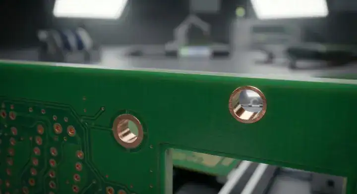
Every production panel requires a 5.0mm to 7.0mm tooling strip (breakaway rail) on the two longest edges to allow SMT machine conveyors to grip the board. Additionally, you must include three 1.5mm diameter fiducial marks—one in each of three corners—to provide the machine with a global alignment reference that accounts for “stretch” or “shrink” in the PCB material.
Many engineers forget that the machine’s “hands” (the rails) need somewhere to hold. If your components are placed right to the edge of the board, the rails will crush them.
- Tooling Rails: Must be free of all components and copper (except fiducials).
- Tooling Holes: Add 3.0mm holes to the four corners of the rails for mechanical mounting in test fixtures.
- Fiducial Clearance: Ensure a 3.0mm “keep-out” zone around every fiducial mark where no copper or silk-screen is present.
Bottom line: Include 5mm tooling strips and 3 global fiducials on every panel design; without them, your CM will likely charge you a setup fee to manually fix the files.
How Does Depaneling Stress Affect Component and Solder Joint Reliability?
Depaneling stress is the mechanical energy transferred into the PCB when boards are separated, with V-score “snapping” generating up to 500 microstrains of force—enough to crack solder joints on BGA or QFN packages. Organizations like SMTA have published data showing that mechanical depaneling is responsible for nearly 15% of all early-life hardware failures.
The method you choose for pcb array for production separation dictates the longevity of your product.
| Depaneling Method | SMT Keep-Out Zone | THT Keep-Out Zone | Connector Keep-Out |
|---|---|---|---|
| V-Score (Hand Snap) | 5.0mm | 7.0mm | 10.0mm (Avoid) |
| V-Score (Machine) | 3.0mm | 4.0mm | 5.0mm |
| Tab-Route (Router) | 1.0mm | 2.0mm | 2.0mm |
| Laser | 0.5mm | 1.0mm | 1.0mm |
Comparison Anchor: Use a mechanical router (Tab-route) if your board contains expensive BGAs or sensitive MEMS sensors. Use V-score only for simple, low-cost boards with large components.
Bottom line: If your design includes 0201 parts or BGAs, spend the extra 5% on Tab-routing; the reduced mechanical stress will prevent thousands of dollars in warranty claims.
Panel Design Checklist: What to Verify Before Sending Files to Your CM
Before you export your Gerbers for pcb panelization for assembly, verify these five metrics: net coverage, fiducial placement, rail width, keep-out clearances, and board-to-board spacing. A final 10-minute check in your CAD tool can prevent a $1,200 stencil re-order fee.
- Verify Global Fiducials: Are there 3 fiducials on the panel rails?
- Check Component Clearances: Are all MLCCs at least 3mm away from V-score lines?
- Confirm Rail Width: Are the tooling strips at least 5mm wide?
- Inspect Tab-Routing: Do “mouse bites” have enough holes (typically 5 holes, 0.5mm diameter) to break cleanly?
- Analyze Symmetry: Is the board layout balanced to prevent reflow warping?
Bottom line: Your panel design is a production tool, not just a layout; treat it with the same engineering rigor as the PCB itself.
Frequently Asked Questions (FAQ)
Which is better for SMT assembly, V-score or Tab-route? It depends on your board shape and component proximity. V-score is better for straight-edged boards and saves material, but it creates higher mechanical stress. Tab-route is better for irregular shapes and sensitive components (like BGAs) because it uses a low-vibration router for separation. Most mass-produced consumer electronics use a combination of both.
How many boards should I put in one panel to save money? The “sweet spot” for most SMT lines is a panel width of 150mm to 250mm. While more boards per panel reduces setup time, going over 300mm increases the risk of warping and sag during reflow, which can actually increase your cost per good board due to defects. For prototypes, a 2-up or 4-up panel is usually sufficient.
What is the minimum component keep-out distance for V-score? You should maintain a minimum of 3.0mm (120 mils) between the center of a V-score line and the nearest SMT component. For larger components or connectors, increase this to 5.0mm. This clearance prevents the mechanical “snap” of depaneling from cracking ceramic capacitors or fracturing solder joints.
Do I need fiducials on the panel if I already have them on the boards? Yes. SMT machines use “Global Fiducials” on the panel corners for initial alignment and “Local Fiducials” on individual boards for fine-tuning. Global fiducials are mandatory for the machine’s vision system to recognize the panel’s orientation on the conveyor belt.
What happens if my panel is too thin? If your panel is thinner than 1.0mm and has a large surface area, it will likely bow or “potato chip” during the reflow process. This causes uneven solder paste thickness and creates open joints. For thin PCBs, we recommend using smaller panels or custom-weighted pallets to maintain flatness.
Optimizing your panel design today prevents the hidden costs of assembly defects tomorrow. At QueenEMS, we offer a free DFM/DFA engineering review on every order to catch these panelization risks before they hit the production line. Whether you are scaling from a 5-unit prototype to a 10,000-unit run, our team ensures your panels are built for maximum yield.
Written by the QueenEMS Engineering Team
Upload your files today · Free DFM check before production · Ship worldwide
Get your PCB prototypes in as fast as 24 hours. We handle FR4, Rogers, and Flex up to 60 layers — free prototypes for 2–4 layer boards, no minimum order.
Just upload your Gerber + BOM — we source every part, assemble, and inspect (AOI + X‑Ray) so you don't have to chase suppliers. Boards ship in as fast as 24 hours.