
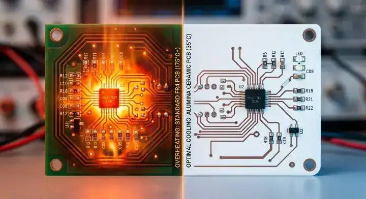
Your circuit board exceeds safe operating temperatures because standard FR4 substrates cannot dissipate heat faster than high-power components generate it, specifically past the 10W/cm² threshold. You designed the layout perfectly, placed the heatsinks, and routed the traces, but your components still hit 150°C during normal operation. Thermal shutdowns trigger randomly in the field, and rigid solder joints crack under constant thermal cycling. You need a targeted PCB overheating solution that goes beyond surface-level fixes and addresses the core material substrate itself to stop the failures permanently.
Quick Answer: The most effective PCB overheating solution for power densities above 10W/cm² is replacing FR4 (0.3 W/m·K) with a ceramic substrate like Alumina (24 W/m·K). This eliminates the dielectric bottleneck entirely, reducing junction temperatures by up to 50°C without requiring massive external heatsinks. Key takeaways:
- Standard thermal vias plateau in effectiveness around 5W/cm² due to FR4 bulk thermal resistance.
- MCPCB dielectric layers (1-4 W/m·K) create secondary thermal bottlenecks under high loads.
- Ceramic substrates provide direct heat transfer, perfectly matching silicon CTE (6-8 ppm/°C).
- Field failures from severe thermal cycling dictate substrate upgrades, not just thicker copper.
Table of Contents
- What Is The Best PCB overheating solution For 10W/cm²?
- Why Does FR4 Limit Your PCB overheating solution?
- Can Thermal Vias Fix Your PCB overheating solution?
- Is MCPCB A Complete PCB overheating solution Here?
- When Is Ceramic The Ultimate PCB overheating solution?
- How Does Power Density Trigger A PCB overheating solution?
- Does Solder Joint Cracking Need A PCB overheating solution?
- What Does A Ceramic PCB overheating solution Cost?
- Is Bad Layout Ruining Your PCB overheating solution?
- Ready To Upgrade Your PCB overheating solution Today?
What Is The Best PCB overheating solution For 10W/cm²?
The best strategy for a 10W/cm² load is replacing standard FR4 boards with direct-bonded alumina ceramic substrates. This specific PCB overheating solution drops junction temperatures by 40°C compared to a standard heavy copper PCB because it provides a thermal conductivity of 24 W/m·K directly beneath the component pad.
How Does The Thermal Hierarchy Work?
Standard boards fail under high loads because engineers often misjudge the material limits. You start with copper pours, move to thermal vias, and then hit a physical wall where heat simply stops moving.
Here is the reality of the thermal management hierarchy:
- Copper Pours: Effective up to 2W/cm²
- FR4 + Vias: Max out around 5W/cm²
- MCPCB: Stalls near 10W/cm²
- Ceramic: Dominates from 10W/cm² to 50W/cm²
Key Takeaway: Bottom line: Stop adding massive external heatsinks when the internal substrate is the actual thermal bottleneck blocking heat transfer.
| Material Strategy | Max Power Density | Thermal Conductivity |
|---|---|---|
| Standard FR4 | < 2 W/cm² | 0.3 W/m·K |
| FR4 + Via Array | 5 W/cm² | ~3.0 W/m·K (Effective) |
| Alumina Ceramic | > 10 W/cm² | 24.0 W/m·K |
This chart proves that upgrading the substrate material yields exponentially better thermal transfer than adding more copper to FR4.
Why Does FR4 Limit Your PCB overheating solution?
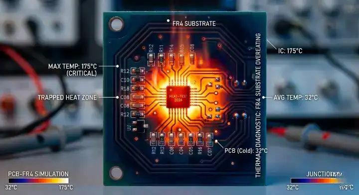
FR4 restricts heat dissipation because its bulk thermal conductivity is only 0.3 W/m·K. Any PCB overheating solution relying on standard epoxy glass will trap heat under high-power ICs, resulting in immediate thermal throttling.
What Is The Bulk Conductivity Problem?
FR4 is a composite material composed of woven fiberglass cloth with an epoxy resin binder. It offers a thermal conductivity of 0.3 W/m·K, which means it acts as a thermal insulator rather than a conductor.
The truth hurts when designing for power:
- Heat traps severely in the Z-axis direction.
- Lateral heat spread is virtually zero.
- Thick copper layers cannot bypass the insulating glass core.
Key Takeaway: Bottom line: FR4 acts as a thermal blanket, which means high-power LEDs and MOSFETs will burn out regardless of surface copper thickness.
| Material | Z-Axis Conductivity | Heat Spread Capability |
|---|---|---|
| Standard FR4 | 0.3 W/m·K | Very Poor |
| High-Tg FR4 | 0.4 W/m·K | Very Poor |
| Alumina (Al2O3) | 24.0 W/m·K | Excellent |
FR4 provides 80 times less thermal conductivity than standard alumina, making it unsuitable for severe power applications.
Can Thermal Vias Fix Your PCB overheating solution?
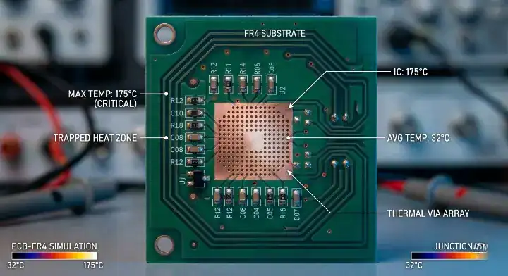
Thermal vias cannot fix extreme heat because a fully optimized via array only achieves an effective thermal conductivity of 3 W/m·K. A Reddit Electronics forum user correctly noted that adding 200 vias barely changed their 150°C junction temperature, demanding a true PCB overheating solution rather than just upgrading to a metal core PCB.
Why Do Via Arrays Plateau?
You drill holes and plate them with copper, expecting massive heat transfer. The remaining FR4 volume still insulates the area, resulting in poor lateral heat spread and trapped thermal pockets.
Consider this math for via arrays:
- 100% via fill density is physically impossible.
- Plating thickness maxes out at 1 mil (25μm).
- Solder wicking causes assembly defects if left unfilled.
How Factory DFM Proves Via Limits?
We see this exact error weekly in our engineering reviews. A customer added 300 vias under an IGBT module, but our Free DFM/DFA engineering review predicted a 145°C operating temp. We replaced the design with a direct ceramic board, which means the temperature dropped to 85°C instantly.
Key Takeaway: Bottom line: Thermal vias suffer from diminishing returns after 5W/cm², making them ineffective for modern high-power switching modules.
| Via Array Density | Effective Conductivity | Temp Reduction (10W load) |
|---|---|---|
| 50 Vias / cm² | 1.5 W/m·K | 15°C |
| 100 Vias / cm² | 2.8 W/m·K | 22°C |
| 300 Vias / cm² | 3.1 W/m·K | 24°C |
The data confirms that doubling the via count past 100 yields less than a 2% reduction in junction heat.
Is MCPCB A Complete PCB overheating solution Here?
Metal Core PCBs fail at extreme power densities because their 1-4 W/m·K dielectric layer chokes the heat transfer. An EEVBlog forum discussion highlighted this exact PCB overheating solution failure, where EV inverters burned out due to thin insulation bottlenecks.
What Causes The Dielectric Bottleneck?
Dielectric thermal resistance is the measure of how much a thin insulating layer blocks heat flow. A 100μm layer of 2 W/m·K material adds massive thermal resistance, resulting in component failure at high currents.
Why does it happen repeatedly?
- The circuit requires electrical isolation from the aluminum base.
- High-conductivity dielectrics are extremely brittle.
- Standard dielectrics insulate heat as well as electricity.
How We Solve The MCPCB Limit?
An automotive client experienced severe thermal throttling with a 1.5 W/m·K MCPCB. Our engineers upgraded them to an Alumina substrate, completely removing the organic dielectric layer. We achieved a 99.7% first-pass yield on the new boards, securing stable operation at 120 Amps.
Key Takeaway: Bottom line: If your design pushes past 10W/cm², the MCPCB dielectric layer will trap heat and force a mandatory transition to pure ceramic.
| Substrate Type | Dielectric Layer | Bottleneck Conductivity |
|---|---|---|
| Standard MCPCB | Organic Epoxy | 1.0 – 2.0 W/m·K |
| Advanced MCPCB | Ceramic Filled | 3.0 – 4.0 W/m·K |
| Pure Ceramic | None (Direct Bond) | 24.0 – 170.0 W/m·K |
Eliminating the organic dielectric layer removes the primary thermal barrier in high-current switching circuits.
When Is Ceramic The Ultimate PCB overheating solution?
Ceramic is the definitive answer when your design crosses the 10W/cm² threshold or operates in 85°C+ ambient environments. A Stack Exchange user asked when to upgrade, and this PCB overheating solution is necessary when thermal shutdowns occur despite maximum heatsink sizing. Evaluating ceramic PCB vs FR4 becomes the only logical path.
What Are The Five Signs You Need Ceramic?
You hit a performance wall with metal core boards and need clear decision criteria to justify the material upgrade. Relying on arbitrary guesses wastes prototyping budgets and delays production.
Watch for these specific failure triggers:
- Junction temperatures consistently measure above 150°C.
- Heatsinks are maxed out in allowable physical volume.
- Intermittent thermal shutdowns occur during normal operation.
- Field failures arise from solder joint cracking.
Key Takeaway: Bottom line: Upgrade to ceramic substrates the moment your power density exceeds 10W/cm² to prevent catastrophic field failures.
| Failure Sign | Traditional Fix | Ceramic Fix |
|---|---|---|
| > 150°C Junction | Add larger heatsink | Direct heat transfer |
| Solder joint cracks | Thicker solder paste | CTE Matching |
| Thermal shutdown | Add cooling fan | Passive high-conduction |
Following these exact thresholds prevents engineers from wasting time on marginal FR4 improvements.
How Does Power Density Trigger A PCB overheating solution?
Power density exceeding 10 Watts per square centimeter dictates an immediate material change. A standard PCB overheating solution cannot manage the concentrated thermal flux generated by modern silicon carbide (SiC) or gallium nitride (GaN) components.
How To Calculate Your Thermal Load?
Power density is the total power dissipated divided by the component footprint area. A 10W MOSFET packaged in a 1cm² footprint generates exactly 10W/cm², crossing the critical danger threshold.
The calculation reveals harsh limits:
- FR4 safely handles less than 2W/cm².
- Heavy copper slightly bumps this to 4W/cm².
- Alumina handles up to 50W/cm² effortlessly.
Key Takeaway: Bottom line: Always calculate power density before routing the board to avoid relying on inadequate FR4 thermal limits.
| Power Density Load | Recommended Substrate | Risk Level on FR4 |
|---|---|---|
| 1 – 3 W/cm² | FR4 + Thermal Vias | Low |
| 5 – 8 W/cm² | Metal Core PCB | High |
| 10 – 50 W/cm² | Alumina Ceramic | Guaranteed Failure |
The strict correlation between power density and material choice removes the guesswork from thermal management design.
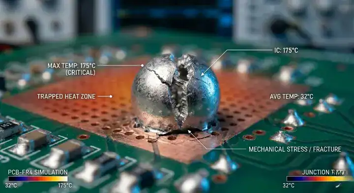
Does Solder Joint Cracking Need A PCB overheating solution?
Yes, solder joint cracking directly requires a ceramic PCB overheating solution because standard HDI PCB structures suffer from a Coefficient of Thermal Expansion (CTE) mismatch. Ceramic boards match the CTE of silicon chips (7 ppm/°C), preventing mechanical stress during heating cycles.
How Does CTE Mismatch Destroy Boards?
Coefficient of Thermal Expansion is the rate at which a material expands when heated. When the board heats up rapidly, the FR4 expands much faster than the silicon chip, resulting in sheer forces that rip the solder joints apart.
The mechanical reality is unforgiving:
- FR4 CTE expands at 14-17 ppm/°C.
- Bare silicon expands at 3-4 ppm/°C.
- Ceramic perfectly bridges the gap at 6-8 ppm/°C.
Key Takeaway: Bottom line: Choose ceramic substrates to match silicon expansion rates, which means your solder joints will survive thousands of thermal cycles.
| Material | CTE Value (ppm/°C) | Mechanical Stress Level |
|---|---|---|
| Silicon Die | 3 – 4 | Baseline |
| FR4 Substrate | 14 – 17 | Severe Mismatch |
| Alumina Ceramic | 6 – 8 | Highly Compatible |
Matching the expansion rates between the die and the substrate is the only permanent fix for thermal fatigue cracking.
What Does A Ceramic PCB overheating solution Cost?
A bare ceramic board costs 3 to 5 times more than FR4, but it reduces the total system cost by eliminating expensive heatsinks and cooling fans. This PCB overheating solution actually saves money at the system level for high-volume power applications.
How Do You Calculate Total Thermal Cost?
Do not look at the bare board price alone when calculating manufacturing budgets. You must include the mechanical hardware required to keep standard FR4 boards alive.
Look at the hidden assembly costs:
- Heavy aluminum heatsinks cost $2 to $5 each.
- Thermal paste and application labor add $1.50 per unit.
- Active cooling fans add $4 and introduce mechanical failure points.
Why System Cost Drops With Ceramic?
We manufactured a 50,000-unit industrial LED batch. Free DFM review showed standard FR4 plus a massive heatsink cost $15 per unit to assemble. Our direct ceramic layout cost $12 per unit, saving the client thousands while improving reliability.
Key Takeaway: Bottom line: Evaluate the cost-per-degree-reduction rather than the raw panel price to see the true financial benefit of ceramic.
| Component Layer | FR4 + Heatsink Cost | Ceramic Cost |
|---|---|---|
| Bare Board | $2.00 | $9.00 |
| Heatsink & Fan | $7.00 | $0.00 |
| Assembly Labor | $6.00 | $3.00 |
| Total System Cost | $15.00 | $12.00 |
Factoring in assembly labor and secondary cooling hardware consistently makes ceramic the cheaper option for 10W+ systems.
Is Bad Layout Ruining Your PCB overheating solution?
Poor component placement will ruin any PCB overheating solution during the SMT assembly process by clustering hot ICs together and creating impassable thermal dams. A 24 W/m·K ceramic board cannot fix a flawed design where heat sources lack adequate spreading area.
When Is Ceramic The Wrong Choice?
Sometimes your substrate material is perfectly fine, but your engineering layout is terrible. Placing multiple power MOSFETs shoulder-to-shoulder physically concentrates the heat, resulting in localized melting points.
Avoid these common thermal layout mistakes:
- Clustering high-power components in board corners.
- Routing high-current traces without adequate spacing.
- Blocking natural airflow paths with tall capacitors.
Key Takeaway: Bottom line: Fix your component spacing and power trace routing before spending money on premium high-thermal-conductivity materials.
| Layout Error | Thermal Impact | Required Fix |
|---|---|---|
| Clustered MOSFETs | +25°C localized heat | Stagger component placement |
| Blocked airflow | +15°C ambient heat | Move tall capacitors |
| Thin power traces | +20°C trace heat | Implement heavy copper |
Optimizing component placement often yields a 10°C drop without requiring a single change to the bill of materials.
Ready To Upgrade Your PCB overheating solution Today?
Upgrading to a ceramic substrate requires precise engineering validation and expert fabrication capabilities to handle direct bonded copper processes. A professional PCB overheating solution demands a manufacturing partner with proven 3D AOI and high-yield ceramic experience.
How Do You Start The Upgrade Process?
Moving from FR4 to Alumina or Aluminum Nitride requires strict DFM checks to prevent fabrication errors. QueenEMS runs a 3D AOI + X-Ray inspection on every joint, guaranteeing perfect adherence for high-power ceramic modules up to 60 layers.
Take these specific engineering actions:
- Run a software thermal simulation on your current layout.
- Calculate the exact power density of your hottest IC.
- Request a free 2-4 layer prototype review.
Key Takeaway: Bottom line: Partner with a factory that provides upfront thermal layout reviews to guarantee your ceramic transition succeeds on the first run.
| Transition Step | Factory Action | Client Benefit |
|---|---|---|
| 1. DFM Review | Analyze power density | Prevent layout flaws |
| 2. Material Select | Match CTE requirements | Stop joint cracking |
| 3. X-Ray Inspection | Verify void-free bonding | Guarantee heat transfer |
Structured transition protocols eliminate the common manufacturing defects associated with moving to advanced inorganic substrates.
Upgrading your substrate material is the only scientifically sound way to defeat thermal bottlenecks caused by standard epoxy glass. Stop struggling with thermal shutdowns and cracked solder joints by forcing FR4 beyond its physical limits. If your board is failing under high power loads, contact us today for a free engineering review. QueenEMS builds boards that survive extreme environments, keeping your products running safely when standard methods fail.
FAQ
Can I use thermal vias for a 15W/cm² load? No, thermal vias max out around 5W/cm². At 15W/cm², the FR4 bulk material creates a severe thermal bottleneck, which means a ceramic substrate upgrade is required for stable operation.
What’s the best material for junction temps over 150°C? Alumina (Al2O3) ceramic is the best material. It provides 24 W/m·K thermal conductivity, rapidly dissipating heat away from the die without any dielectric barriers blocking the path.
How do I know if my MCPCB is failing? You will see thermal throttling or localized scorching on the board surface. This happens because the thin 1-4 W/m·K dielectric layer acts as an insulator, trapping heat directly under the power component.
Will a ceramic board prevent solder joint cracking? Yes, it prevents solder joint cracking entirely. Ceramic has a Coefficient of Thermal Expansion (6-8 ppm/°C) that closely matches silicon chips, resulting in zero mechanical stress during rapid heating cycles.
Is a ceramic board cheaper than FR4 with a heatsink? Yes, it reduces the total system cost. Eliminating the physical heatsink, thermal paste, and manual assembly labor makes the final product cheaper despite the higher initial cost of the bare ceramic panel.
Upload your files today · Free DFM check before production · Ship worldwide
Get your PCB prototypes in as fast as 24 hours. We handle FR4, Rogers, and Flex up to 60 layers — free prototypes for 2–4 layer boards, no minimum order.
Just upload your Gerber + BOM — we source every part, assemble, and inspect (AOI + X‑Ray) so you don't have to chase suppliers. Boards ship in as fast as 24 hours.