Quick Answer: Specify a PCB busbar as a conductor with defined board connections, supports and load taps. Check the copper between each tap and its load, and approve the joining process on the intended bar-board assembly. Bare-board continuity and bar dimensions provide useful evidence; current-carrying performance needs a test of the connected construction under stated conditions.
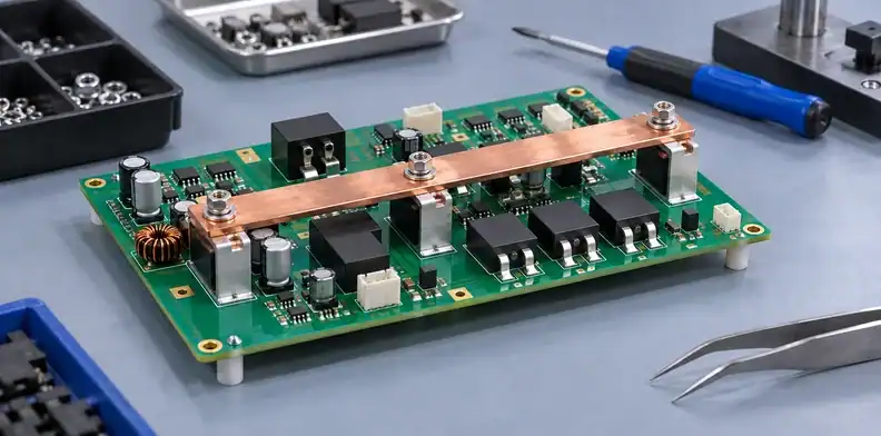
A PCB busbar can move a power rail across a board without making the entire route an etched copper trace. Purchasing the copper bar is only part of the decision. The connections at its ends and taps determine how current enters the PCB, while the mounting arrangement determines where cable and assembly forces go.
An order that says “PCB with high-current busbar” leaves several different deliverables unresolved. Does the supplier provide the board, the formed conductor, an installed assembly or a tested assembly? Establish that boundary before releasing the footprint.
Table of Contents
- Locate the busbar in the complete current path
- Choose the joint before designing the footprint
- Pair the bar drawing with the PCB drawing
- Check the copper that remains after the bar
- Find joint heating with a bounded resistance review
- Give the assembly a deliberate load path
- Specify the contact surface and insulation boundary
- Plan the joining process around the metal mass
- Qualify the connected assembly at defined conditions
- Quote the PCB and busbar work as separate deliverables
Locate the busbar in the complete current path
Identify where current enters the bar, where it leaves and how it returns to the source. A PCB busbar may carry the main supply across a board, distribute it to several loads or connect an external cable to a board region. Those arrangements place different demands on the connections.
Draw the conductor as its own part in the power-path sketch. Mark the infeed, load taps and any sense-only connections. Give each segment its intended operating current, including the states in which several loads run together. A nominal system current alone does not describe the current at every pad.
Consider a bar crossing a control board while most load current continues to another assembly. A small connection to voltage-sensing circuitry has a different duty from a connection supplying a power stage. Its position on the same bar does not make it a full-load connection.
The return path also belongs in the sketch. Replacing a supply trace with a bar leaves the return conductor, connectors and load-side copper to be reviewed. The large-board feed and return discussion covers that wider distribution decision; here the sketch establishes which physical interfaces need approval.
Keep thermal inserts identifiable by their actual function. A local copper coin under a device and a mounted electrical busbar can both contain substantial copper, but they have different interfaces and acceptance questions. Show the intended electrical connections explicitly, including any portion of the conductor that remains isolated from board circuitry.
Choose the joint before designing the footprint
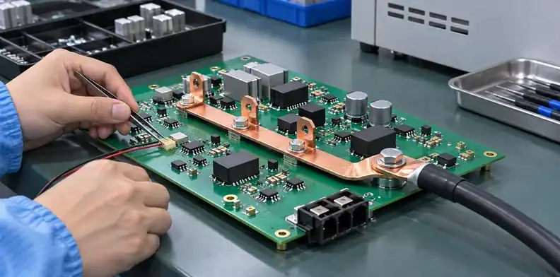
Select a joining system with defined mating surfaces and assembly requirements. A soldered tab, a bolted contact and a specified press-fit element require different PCB features. The footprint should follow the chosen system and its documentation.
Amphenol’s PCB busbar product description lists formed copper tabs and wave-soldered or bolted installation options. This establishes available construction choices within that offering. It supplies no general current rating or interchangeable assembly recipe.
| Connection approach | PCB feature to resolve | Assembly detail to approve | Evidence needed for the project |
|---|---|---|---|
| Soldered through-hole tab | Finished opening, surrounding land and copper connection | Tab fit, solder access and support during joining | Trial joints on the proposed geometry |
| Broad soldered contact | Land geometry, mask boundary and adjacent clearance | Placement, solder quantity and heating method | Joint inspection and a defined loaded trial |
| Bolted contact | Contact land, clearance opening and support arrangement | Hardware stack, mating surfaces and tightening method | Contact performance with the specified hardware |
| Named press-fit system | Supplier-specified finished-hole and board construction | Insertion tooling, support and applicable force limits | Evidence for the actual element-board combination |
Soldered tabs and broad contact lands
For a soldered tab, distinguish the metal tab dimensions from the finished PCB opening. Record the geometry that controls fit and the surfaces intended to wet. A contact that spans a large land also needs a clear placement boundary so solder spread does not reach adjacent circuitry.
Ask the assembler how the bar will remain in position during joining. An electrically adequate land can still be difficult to process when the conductor tilts, traps access or moves as the fixture heats.
Bolted and specified press-fit interfaces
A bolted interface needs a defined contact plane and hardware stack. Identify where the clamp load is reacted and which surfaces carry current. A mounting bolt through an insulated hole may provide support without forming an electrical connection.
For press-fit, use the selected element manufacturer’s requirements. The finished-hole approval method explains why a nominal drill diameter cannot establish compatibility. Keep generic holes and controlled press-fit holes in separate drawing classes.
Pair the bar drawing with the PCB drawing
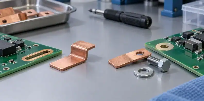
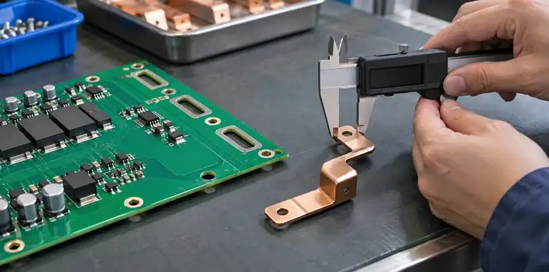
Release the conductor and PCB drawings as a matched pair with common reference features. Each supplier may manufacture its own part correctly while the two parts fail to mate because their offsets, datums or tolerance assumptions differ.
Begin with the feature that locates the bar on the assembly. It might be a board datum, a chassis mounting point or a defined contact plane. Dimension the corresponding PCB features from an agreed reference, and show the bar’s orientation relative to that reference.
| Interface feature | Conductor drawing | PCB drawing |
|---|---|---|
| Position and orientation | Locating feature and direction of the formed part | Matching datum and component outline |
| Tab or pin fit | Finished metal dimensions and applicable finish | Finished opening size, shape and hole class |
| Bolted electrical contact | Mating face, opening and hardware arrangement | Contact land, clearance opening and support area |
| Vertical position | Formed offset and contact-plane relationship | Finished board thickness and nearby height restrictions |
| Insulated clearance | Insulation boundary and exposed regions | Copper, component and board-edge keepouts |
Use finished dimensions where the parts physically mate. The bar drawing should clarify whether a tab dimension includes its coating. The PCB drawing should identify whether an opening is plated and which finished size governs fit.
A flat tab through an elongated opening also needs a controlled slot shape. The plated-slot drawing requirements address that feature. Do not substitute a round-hole callout while leaving the assembler to discover the difference.
Include an assembly view that shows access around the joint. A bar may fit the bare board yet prevent a socket, solder nozzle or inspection tool from reaching the connection after nearby parts are installed. Review the assembly sequence against the same geometry before approving both drawings.
Check the copper that remains after the bar
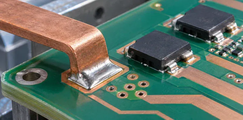
Follow each tap from the busbar connection to its load terminal. That path may contain a pad neck, an outer-layer trace, vias and an inner-layer segment. The bar carries current only along its own route; the remaining PCB copper still performs its assigned work.
In an illustrative distributed-load arrangement, several power stages connect along a common bar. Each local branch should be reviewed for its branch current and operating state. Do not assume equal current sharing merely because the branches look similar on the board.
Check the conductor transition at each tap. A wide contact land can connect to a much narrower copper neck, and a via group can transfer current to a layer with a different geometry. Mark these transitions on the layout so the review follows the physical path instead of stopping at the footprint outline.
The heavy-copper pattern and stack discussion supports copper selection where substantial board current remains. Use the actual width, finished copper, temperature boundary and duty for this project; a copper-weight label by itself supplies no complete branch rating.
A sensing-only tap offers another useful review case. Its normal current may be small, but its placement and protection still depend on the circuit. Keep that connection separate from the load-tap specification so a supplier does not infer identical pad requirements for every position.
Confirm the return connections at the same time. A substantial supply bar paired with an unresolved return neck can leave the distribution path constrained at a location that is easy to overlook during conductor purchasing.
Find joint heating with a bounded resistance review
Separate the voltage drop along the bar from the drop across its connections. A measurement over the complete route can identify a loss problem while hiding whether it belongs to the bar, one contact or the adjoining PCB copper.
Separate the drop across each connection
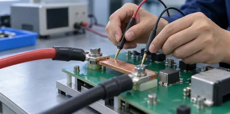
Define voltage-sense locations around the segment being assessed, and record the current through that segment. At steady conditions, its resistance follows from the measured voltage drop divided by current. Include the sense-point positions in the test record so another sample can be measured over the same physical boundary.
For a contact assessment, sense points that extend far into the copper track include track resistance. A changed probe location can then resemble a changed joint. Keep the current leads and voltage-sensing arrangement identified, and account for instrument resolution and lead/contact effects in the chosen method.
An infrared view can help locate surface heating, but its interpretation also depends on the observed surface, camera setup and access. Record the temperature method and locations. Do not translate a bright image patch into a measured contact resistance.
An illustrative joint-loss calculation
The following assumptions demonstrate how to apportion loss. They are invented design-review values, not measurements or ratings for a QueenEMS board.
| Assumed segment at 100 A | Assumed resistance | Calculated drop, V = IR | Calculated heat, P = I²R |
|---|---|---|---|
| Bar between its connection regions | 0.10 mΩ | 10 mV | 1 W |
| Infeed connection | 0.25 mΩ | 25 mV | 2.5 W |
| Outgoing connection | 0.25 mΩ | 25 mV | 2.5 W |
| These three segments together | 0.60 mΩ | 60 mV | 6 W |
Under these assumptions, the two connections account for five of the six watts. Increasing the bar’s copper cross-section would address only the bar’s one-watt contribution. The review should therefore investigate the specified contacts, joining process and local heat path as well as the conductor.
Actual temperatures require the real assembly, losses and thermal boundary. The arithmetic does not establish an allowable current or predict a temperature rise.
Give the assembly a deliberate load path
Identify where installation and service forces are reacted. A cable, fastener or insertion tool can impose a mechanical demand on the PCB connection even when the electrical route appears adequate.
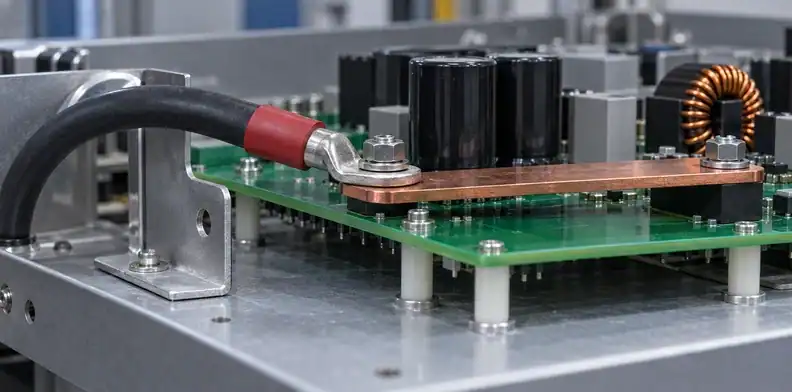
The support arrangement should be visible in the assembly drawing. Show the standoffs, brackets or chassis interfaces that carry the intended loads, and identify which connection regions require access from below. Review the unsupported spans of both the bar and board.
| Situation to review | Mechanical question | Proposed design or trial evidence |
|---|---|---|
| Cable attached at the bar end | Where does cable force enter the structure? | Installed cable routing and support view |
| Bolt tightened near the board | What reacts the clamp and tool forces? | Hardware section and assembly fixture arrangement |
| Press-fit insertion | Is the relevant board area supported during insertion? | Tooling plan for the selected system |
| Bar spanning several mounting points | Can relative movement load its contacts? | Tolerance review and intended exposure trial |
| Service access | Can a tool disturb nearby joints or components? | Assembly and removal sequence check |
A copper bar can also constrain the board when its mounting points prevent relative movement. Evaluate the actual offsets, materials and operating exposure with the mechanical designer. Avoid assuming that extra stiffness automatically improves the reliability of every connection.
Keep energized metal clear of board edges, fasteners and neighbouring circuits through the permitted movement range. The copper-to-edge geometry review covers the board feature; the installed bar and hardware add their own clearance envelope.
For a cable-fed prototype, inspect the assembly with the intended cable present. A small unconnected bar on a bench omits cable weight, bend stiffness and the connector access that may dominate the mechanical review.
Specify the contact surface and insulation boundary
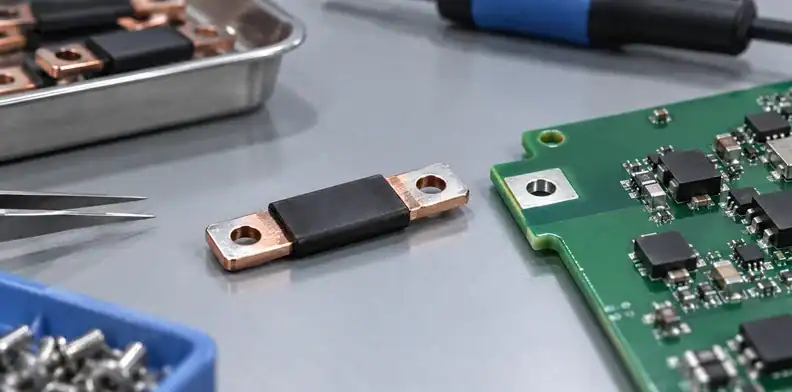
Assign finish requirements to the regions that actually join or contact another part. A busbar drawing may contain exposed contact faces, soldered tabs, insulated spans and mounting surfaces, each with a different purpose.
Mersen’s busbar design guide treats conductor finish as part of the electrical connection and separately describes mounting and insulation. Its scope is laminated busbars. Identify the contact surfaces on the supplied conductor; assess PCB assembly capacity from the actual connected construction.
On the conductor drawing, mark the mating faces and insulation boundaries. State the offered finish system and which surfaces it covers. Resolve whether the bar supplier or assembler prepares the interface, and preserve any handling or storage requirements associated with the selected joining system.
On the PCB, identify the solder-mask boundary and exposed land. A plated board land and a plated bar face have to function together under the selected process. The finish names alone do not establish the assembled resistance or resistance stability after the intended exposure.
Consider an insulated bar span with exposed end contacts. A shifted insulation boundary may reduce tool access or leave unintended metal near another circuit. Review that boundary against the assembled clearances and contact geometry, including its manufacturing variation.
Approve changes to the contact system explicitly. Substituting a finish, cleaning method or mating hardware can alter the interface being evaluated. Keep those revisions with the bar-board assembly record.
Plan the joining process around the metal mass
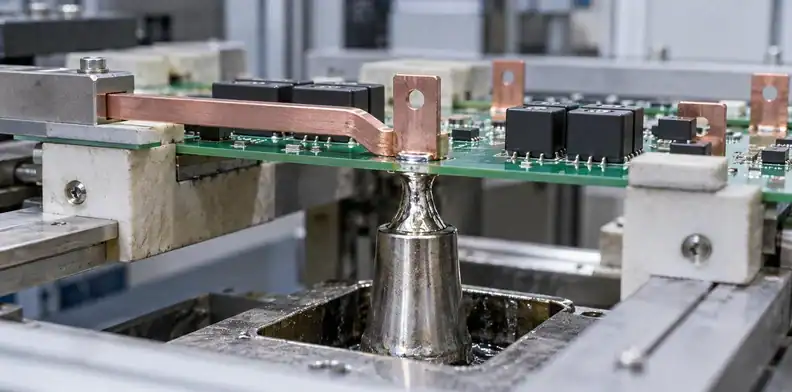
Ask the assembler to assess the selected joining process using the actual bar, PCB and fixture. A large metal conductor changes the heating task around a soldered joint, while a bolted or press-fit connection introduces different tooling and support requirements.
For soldering, agree how the joint receives heat, how the assembly is supported and how the result will be inspected. The trial should include the specified conductor dimensions, finished PCB features and nearby components that affect access. A small solderability coupon cannot reproduce all these conditions.
Use the bare-board solderability evidence to assess the supplied board surface when applicable. Add a joining trial to evaluate the bar-board geometry, with an agreed inspection method and acceptance criteria. These records answer different questions.
The assembly order deserves a physical review. Installing a high bar before nearby components may block later operations; installing it afterwards may obstruct tooling at its own contacts. A fixture that holds the conductor accurately should also permit the heating, insertion or tightening operation.
Record the joining materials, equipment settings and support conditions used in approved trials. Require review when a production proposal changes a feature that the trial represented. Examples include a different bar thickness, hardware stack, PCB finish or inaccessible fixture support.
For separately supplied boards and conductors, define how mismatched or damaged parts are handled before joining. An assembler should have a clear route for reporting a fit discrepancy while both parts remain traceable to their drawings.
Qualify the connected assembly at defined conditions
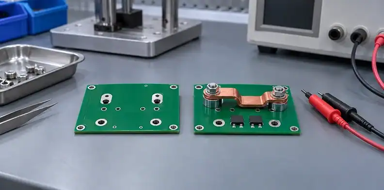
Request evidence at the stage where the relevant interface exists. Board fabrication records establish specified board features. The installed bar, contacts and mounting hardware need their own acceptance and qualification scope.
| Evidence item | What it can establish within its scope | Additional work for the busbar interface |
|---|---|---|
| Bare-board electrical test | Continuity and isolation against the board test data | Check the bar and connections after assembly |
| Board dimensional report | Finished holes, thickness and inspected geometry | Verify conductor fit and installed position |
| Representative board microsection | Selected copper, plating and laminate features | Assess the separately formed joint or contact |
| Loaded assembly trial | Drop and heating at stated operating conditions | Repeat for the required states and boundaries |
| Defined environmental exposure | Behaviour of the tested assembled specimen | Evaluate relevant changes and agreed post-exposure checks |
What the bare board can establish
Keep the fabrication electrical-test scope tied to the board netlist and shipment. Where an external bar later connects separate copper regions, explain that assembly connection in the electrical documentation.
A representative PCB section report can support the relevant board features. It cannot establish the resistance of a bar that has not yet been installed.
When separate terminal regions remain unconnected until the bar is fitted, show that condition in the fabrication data and assembly instructions. The board test programme and the assembled test programme then have different expected connections. Resolve that difference before a receiving team interprets an intentional bare-board separation as a defect.
What needs the bar and its hardware installed
Define operating current, load distribution, ambient conditions, airflow and mounting arrangement for the loaded trial. Record voltage-sense locations and temperature locations, together with the bar, board and process revisions. Set acceptance limits through the product requirements and the agreed test plan.
For exposure testing, identify the specimen construction and what is checked afterwards. A result from one hardware stack or joining process supports that tested configuration. Changing the contact finish, support or process requires a review of which evidence still applies.
Quote the PCB and busbar work as separate deliverables
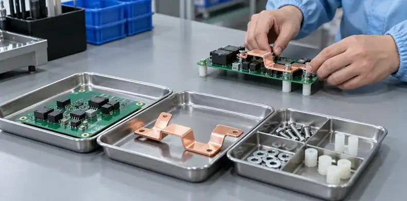
Ask quotations to identify the board, formed conductor, hardware, joining work and evidence as distinct scope items. A low board price and a complete installed-assembly price are not comparable until those boundaries are visible.
Provide matched drawings, the electrical route with tap duties and the intended mounting arrangement. Include the selected joining system, conductor finish and insulation regions. State whether parts arrive separately or whether the order includes the installed bar-board assembly.
List pilot quantities and any specimens consumed by inspection or qualification separately from production quantities. Ask which joining trials and reports are included, who supplies the conductor and hardware, and who approves the assembled interface. QueenEMS capability for a particular conductor or process should be confirmed during project review.
For repeat orders, retain the approved board and conductor revisions together. A board revision that moves a mounting feature or a conductor substitution that changes a contact can affect an otherwise familiar assembly. Identify the approval needed before either supplier implements that change.
Send the paired conductor and PCB drawings, tap-current sketch, mounting view and proposed joining/test scope through the QueenEMS project inquiry. Request a quotation that states the offered parts, assembly responsibilities and any unresolved interface assumptions.
Sources
Written by the QueenEMS Engineering Team
Upload your files today · Free DFM check before production · Ship worldwide
Get your PCB prototypes in as fast as 24 hours. We handle FR4, Rogers, and hybrid boards up to 40 layers in volume production, with advanced builds subject to engineering review — free prototypes for 2–4 layer FR-4 boards, no minimum order.
Just upload your Gerber + BOM — we source every part, assemble, and inspect (AOI + X‑Ray) so you don't have to chase suppliers. Boards ship in as fast as 24 hours.