
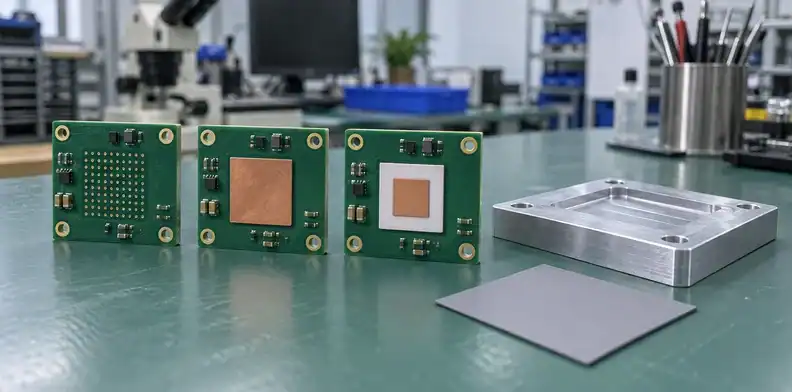
Quick Answer: SiC MOSFET PCB cooling starts with the package heat path and the electrical potential of its exposed pad. Thermal vias and a copper coin can carry both heat and the pad’s voltage toward the board backside, so the cold-plate interface may need a separately qualified insulating layer. An aluminum nitride insert can put an insulating material in the local heat path, but its metallization, bonded interfaces and edge distances still require review.
SiC MOSFET PCB cooling can improve while the electrical isolation becomes worse. Replacing a via field with solid copper reduces one thermal restriction, yet it can also bring a live drain conductor closer to a grounded cooler. A drawing that shows only the new metal cannot establish whether the assembled converter is safe or cool enough.
This article addresses packaged, discrete silicon carbide MOSFETs mounted on a multilayer organic board. The decision is whether to retain thermal vias, use a conducting copper insert, or investigate a ceramic insert beneath a bottom-cooled device. Start with the device and the system’s isolation requirement, then compare complete paths to the same cooler boundary.
Table of Contents
- Identify the cooling surface and its electrical potential
- Give SiC MOSFET PCB cooling a loss and temperature budget
- When can a via array carry the heat?
- A copper coin moves the isolation to another interface
- Where an AlN insert changes the design
- Check insulation through, around and beyond the insert
- Work through a board-to-cold-plate bottleneck
- Reflow and clamping can erase the thermal gain
- Validate temperature, switching and insulation together
- Quote the device, heat path and isolation stack together
Identify the cooling surface and its electrical potential
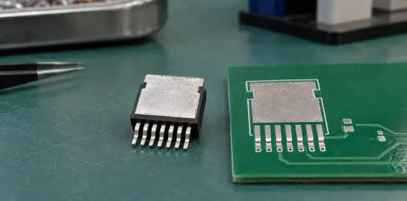
Confirm the cooling surface and its net from the exact device datasheet before connecting a thermal feature. A large metal pad does not automatically belong to ground, and the same package name does not establish an identical pin arrangement across manufacturers.
For a concrete example, Wolfspeed’s C3M0032120J1 datasheet identifies the TO-263-7 XL drain connection and separates the driver-source connection from the power source. Use that device’s pin configuration and recommended land pattern when reviewing its footprint. Other parts need their own checks. C3M0032120J1 datasheet
| Package construction | First document to check | Consequence for the PCB cooling decision |
|---|---|---|
| Bottom-cooled surface-mount device | Pinout, exposed-pad identity and bottom thermal reference | Board metal beneath the pad may also carry its electrical potential |
| Purpose-built top-cooled surface-mount device | Top thermal-contact drawing and assembly instructions | The intended primary heat path can bypass the board thickness |
| Through-hole device with an exposed tab | Tab connection and mounting specification | The tab-to-heatsink interface needs its own electrical and mechanical design |
| Factory-isolated package or module | Explicit insulation rating and its conditions | Apply the documented rating to the specified construction; retain external spacing checks |
Mark the pad, via field or insert with its net on the local section drawing. In a half-bridge, different drains can belong to the DC bus and switching node. Connecting both to one uninsulated cooler can join conductors that the schematic keeps separate.
Adding a ceramic plate above the plastic body of an ordinary bottom-cooled part does not create a purpose-built top-cooled package. Verify where heat leaves the package before adding material. A design based on bare dies or a full ceramic power module follows a different route; ceramic substrate choices for IGBT and SiC modules address that architecture.
Give SiC MOSFET PCB cooling a loss and temperature budget
Calculate the resistance available between the junction and the specified cooler temperature using device loss and a chosen junction-temperature target. Converter output power is not the heat generated in one transistor.
Use the circuit’s conduction loss, switching loss and relevant reverse-conduction intervals at the operating points being evaluated. Record the switching frequency, gate drive, load and temperature assumptions. A loss estimate made at room temperature may need another iteration when the proposed cooling arrangement changes the operating temperature.
| Budget input | What to identify | Mistake that changes the answer |
|---|---|---|
| Device dissipation | Loss of each switch at the evaluated operating point | Dividing converter power equally among devices |
| Junction target | Design target with the project’s chosen margin | Treating absolute maximum temperature as the desired operating temperature |
| Cooler boundary | Temperature at the mating cold-plate surface | Substituting inlet coolant temperature without its intervening path |
| Package term | Correct junction-to-case value and case surface | Combining a top-surface measurement with a bottom-case resistance |
| Board and interface terms | Solder, through-board path, dielectric and contact resistances | Comparing a bare coin with a complete via-to-cooler assembly |
For steady operation, a preliminary allowance is Ravailable = (Tjunction target − Tcooler surface) / Pdevice. Subtract the package and other known terms to find the allowance for the board and insulating interface. This is a screening model; parallel heat paths and three-dimensional spreading can require a fuller model.
TI’s thermal-metrics note explains why a datasheet junction-to-ambient resistance changes with the test board and environment. It also distinguishes a thermal resistance from a characterization parameter used to estimate junction temperature. Match the metric to the measurement location before accepting a temperature prediction. Semiconductor and IC Package Thermal Metrics, Rev. D
Overload pulses need the relevant transient thermal impedance and time history. Keep those calculations separate from the continuous-duty budget. Copper thickness is another explicit model input; the differences among 1 oz, 2 oz and 3 oz board copper help describe the conductor being quoted.
When can a via array carry the heat?
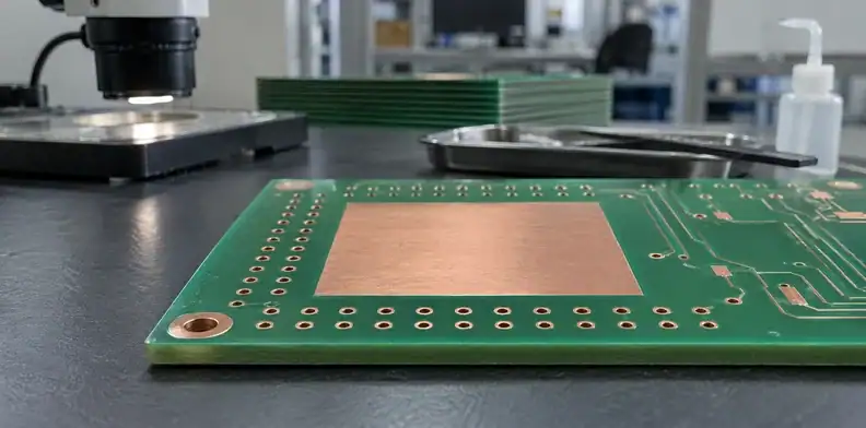
Retain a via-based design when the actual copper planes, plated barrels and cooler interface meet the thermal budget with an acceptable assembly process. Via count alone cannot answer that question.
Copper barrels and spreading planes
Heat must reach the barrels through the surface copper, travel through the available metal and leave through the backside structure. An antipad on an unrelated inner plane prevents an electrical connection to that plane; it also changes the available spreading path. The thermal model should represent the fabricated stackup and clearances.
Infineon’s AN-2021-02 experiments varied board layers, copper thickness, via dimensions, matrix size and heatsink arrangements for TO-263 SiC devices. That is evidence for evaluating the combined construction rather than copying a single matrix from an unrelated board. Its test setup is not a universal resistance value for every SiC footprint. Thermal measurement for D2PAK on PCB
Keep solder out of unfinished holes
Open holes inside the drain solder land can draw solder during reflow. Agree the via treatment and paste design before using that arrangement. Moving vias outside the land avoids one direct solder-wicking path but adds lateral travel through the surface metal.
Resin-filled and copper-filled holes have different interiors. Neither the word “filled” nor a flat-looking surface establishes the amount of metal through the board. The distinction between copper fill and resin fill in via-in-pad builds helps turn that choice into an unambiguous fabrication note. Keep all connected metal on the intended pad net.
A copper coin moves the isolation to another interface
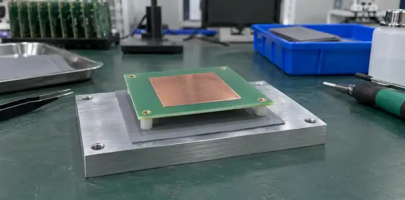
A coin connected directly to a live drain pad remains a live conductor. Its lower through-board resistance can make the insulating layer between the coin and cooler the next thermal restriction.
Review a continuous section from the device pad to the cooler. Show where the coin ends, where the electrical barrier begins and how the cooler is referenced. A soldered metal attachment and an insulating adhesive attachment are different electrical architectures even if their external shapes look similar.
| Local heat-transfer option | Electrically conducting path | Where insulation must be resolved | Selection trigger |
|---|---|---|---|
| Plated via field | Pad, connected barrels and selected copper layers | Board-to-cooler stack and neighboring nets | The complete assembly fits its temperature allowance |
| Copper coin bonded to the pad | Pad and coin, subject to the actual connection | A dielectric interface or another explicitly designed barrier | Board resistance constrains the via design and the remaining barrier is feasible |
| Metallized AlN insert | Top and bottom metallization remain separate if the construction preserves that separation | Ceramic bulk, edges and adjoining interfaces | Thermal transfer and local insulation must be addressed in the same region |
The table compares electrical paths; it does not rank qualified products. A high-conductivity coin may perform poorly if its contact area is small or its insulating foil is thick. A ceramic insert may also lose its advantage through bonding layers or an incomplete backside contact.
Generic cavity fit, surface height and fabrication acceptance belong in the embedded copper coin manufacturing and acceptance discussion. For this application, the additional drawing requirement is a named electrical boundary between the drain-connected structure and every cooler or chassis conductor.
Where an AlN insert changes the design
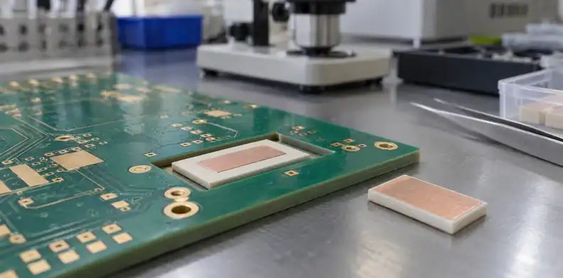
An aluminum nitride, or AlN, insert can carry heat through an electrically insulating ceramic body while the surrounding organic board retains multilayer routing. Its usefulness depends on the complete insert assembly.
Wolfspeed has published an embedded-AlN approach with ceramic between top and bottom copper pads. That construction places insulation within the through-board heat path. It is a different proposal from putting a ceramic sheet against the molded top of a conventional bottom-cooled package. The published geometry and results describe that study, not a guaranteed result for another footprint or supplier. Thermal Solutions for Surface Mount Power Devices
Specify the ceramic grade and dimensions, metallization on each face, attachment materials and permitted edge condition. The upper metallization can carry drain potential while the bottom metal faces the cooler. Conductive wraparound plating, a metal fastener or contamination at an exposed edge can change the intended separation.
Kyocera identifies both thermal conduction and electrical insulation as AlN properties. Those material properties do not assign an equipment insulation rating to a bonded insert. A grade’s conductivity also cannot describe the resistance of its solder, adhesive and cooler contacts. The relationship between ceramic conductivity and assembly resistance is useful when reviewing a supplier’s thermal comparison.
Ask for the proposed integration process before selecting this route. It may introduce a specialist fabrication or assembly step. A request for quotation should distinguish a candidate architecture from an already approved manufacturing process.
Check insulation through, around and beyond the insert
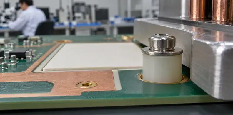
Review solid insulation, surface creepage and air clearance as separate paths in the assembled product. The shortest path may be beside the insert or near a mounting screw rather than through its center.
Solid dielectric and interface edges
The system engineer needs the applicable equipment requirements, working voltage, transients, insulation function, pollution conditions and altitude. Use those inputs to establish dimensions and verification conditions. A material’s breakdown-strength value alone cannot set the board’s safety spacing.
| Path being reviewed | Physical feature to inspect | Information needed before approving it |
|---|---|---|
| Through the insulating material | Minimum thickness, damage and local compression | Material identity and the required electrical test conditions |
| Along its surface | Metallization setback, exposed edge and contamination | Required creepage and applicable material/environment classification |
| Through air | Coin edge, terminal, clamp or screw to cooler metal | Required clearance and peak-voltage/altitude conditions |
| Around the local footprint | Inner planes, neighboring devices and board cutouts | Full net geometry and actual fabrication tolerances |
A cooler drawing should show the protruding features that approach the drain-connected metal. An insulating pad’s nominal outline is insufficient when positioning tolerance or clamping changes its exposed margin. The ceramic dielectric-strength review for power modules develops the material and assembly evidence behind those insulation claims.
Switching capacitance to the cold plate
An intact dielectric still has capacitance. Increasing live metal area or reducing the separation can increase coupling to a grounded cold plate. As a first approximation, displacement current follows I = C × dv/dt; a switching node can therefore inject current through a barrier that passes a DC insulation test.
Include the insert geometry and cooler reference in the switching and electromagnetic-interference review. Retain the package’s Kelvin-source routing and gate-loop design when changing thermal copper. A board revision should undergo electrical review even when its stated purpose is cooling.
Work through a board-to-cold-plate bottleneck
A simple conduction calculation can show which part of the proposed path deserves a prototype. It cannot qualify isolation or predict the finished converter’s junction temperature by itself.
An illustrative conduction comparison
Consider an illustrative bottom-cooled footprint with 60 mm² of effective heat-transfer area on a 1.6 mm board. Assume 20 W of device loss, a 70°C cooler mating surface and a 120°C junction design target. The available junction-to-cooler allowance is (120 − 70) / 20 = 2.5 K/W. These are chosen calculation inputs, not measured customer or QueenEMS results.
For an ideal uniform slab, use R = t / (k × A), with thickness in meters, conductivity in W/(m·K) and area in square meters. Assume copper conductivity of 380 W/(m·K) for this example. A solid copper path through the 1.6 mm thickness gives 0.0016 / (380 × 60 × 10⁻⁶), or approximately 0.070 K/W.
Now add an illustrative insulating sheet with 0.5 mm thickness and assumed conductivity of 3 W/(m·K) across the same area. Its bulk term is approximately 2.78 K/W. Coin plus sheet already reaches about 2.85 K/W before adding the package, solder and contact resistances. The copper path looks attractive in isolation, but this particular insulating stack exceeds the entire preliminary allowance.
For comparison, assume 32 hollow plated barrels with a 0.30 mm finished inner diameter and 0.035 mm radial copper thickness. Their combined metal cross-section is 32 × π × [(0.15 + 0.035)² − 0.15²], approximately 1.18 mm². Treating only those barrels as parallel straight conductors gives approximately 3.57 K/W. This deliberately omits surrounding laminate and other heat paths, as well as spreading and contact resistance; it is not a complete via-board prediction.
Use the calculation to choose a prototype
An illustrative ceramic block of the same thickness and 60 mm² area, with assumed conductivity of 150 W/(m·K), has a bulk term near 0.18 K/W. That result makes a ceramic path worth investigating; its bond layers, metallization, edge insulation and cooler contact remain uncalculated. The arithmetic cannot justify replacing the whole interface with an unqualified ceramic assembly.
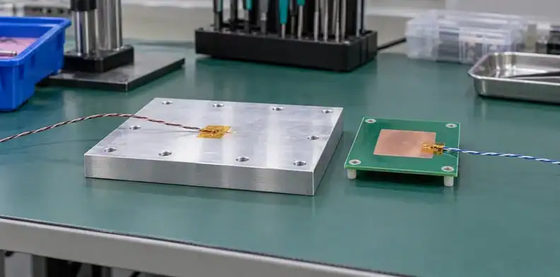
The next experiment should distinguish a through-board restriction from an insulating-interface restriction. Compare samples with the same device, loss, cooler temperature and mounting conditions. Measure the local pad-to-backside drop and the backside-to-cooler drop using a justified sensor arrangement. Preserve the required electrical barrier in every sample.
A thinner insulating sheet might lower resistance, but the system’s insulation requirement must permit the changed material and thickness. Alternatively, a larger effective interface area, revised cooler contact or purpose-built top-cooled package may deserve evaluation. Choose the prototype that addresses the calculated restriction, then use measurements to replace the assumptions.
Reflow and clamping can erase the thermal gain
Verify the drain-pad joint and cooler contact on the real assembly because gaps and loading change the path calculated from bulk materials. A promising board section still needs a repeatable assembly sequence.
More metal beneath a solder land changes its heating behavior during reflow. Instrument the relevant joint on representative boards and review paste volume, wetting and the package’s specified reflow limits. A thermal profile measured elsewhere on the panel does not establish the temperature history of this joint. The reflow profile investigation for SMT defects covers the process review behind that measurement.
Inspect the large solder interface for the agreed defect conditions rather than accepting a visually sound perimeter as proof of full contact. Select inspection that can resolve the suspected defect; an X-ray image, section or other method answers a different question from surface appearance. Avoid declaring a universal acceptable void percentage without a device, location and acceptance basis.
On the cold side, document the dielectric’s compressed thickness, cooler flatness and assembly load path. Clamps should transfer force through the intended mechanical supports. A ceramic insert needs particular attention to edge contact and concentrated force; a conductive coin also needs control of how its height affects the neighboring board and solder joint.
For repeat builds, keep the thermal-interface material and installation method identifiable. A purchasing substitution that preserves nominal conductivity but changes thickness, compression or electrical rating can alter the evaluated construction. Recheck the affected interface before approving that replacement.
Validate temperature, switching and insulation together
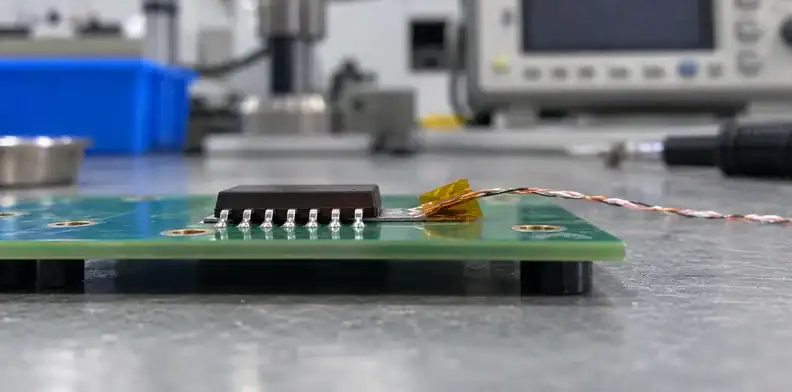
Demonstrate thermal, switching and insulation behavior on the same proposed construction, while keeping the test for each mechanism distinct. Bare-board electrical continuity cannot demonstrate the assembled device’s temperature or isolation to its cooler.
| Verification task | What the specimen must contain | Result to compare |
|---|---|---|
| Thermal performance | Device attachment, board path, dielectric and actual cooler contact | Temperature rise at stated loss and cooler boundary; calibrated junction estimate when required |
| Switching behavior | Actual gate driver, return routing and DC-link layout | Gate/drain waveforms, overshoot and behavior at the operating extremes |
| Isolation to the cooler | Intended barrier, edges, mounts and relevant metalwork | Results under the equipment’s specified voltage, duration and environment |
| Interface durability | The solder, insert and mounting interfaces being qualified | Changes in contact, structure and thermal behavior after the defined exposure |
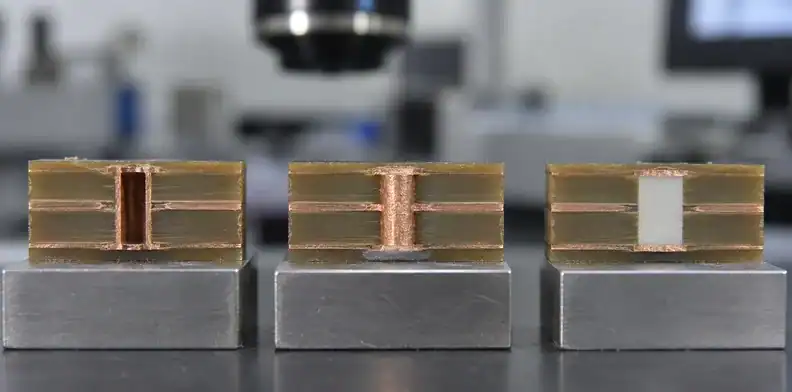
| Fabricated local construction | A representative section or appropriate coupon | Dimensions, connected copper and layer/interface identity against the released drawing |
Attach test conditions to every thermal result: dissipation, sensor location, cooler temperature, mounting pressure or load, interface material and surrounding heat sources. An infrared image of the package surface is useful for locating hot regions, but it is not automatically a junction-temperature measurement. Use a package-appropriate method and record how the estimate was obtained.
Prototype review also needs the actual fabricated local stack. A PCB microsection report can document a selected cross-section, but it cannot establish every feature in an entire assembly. Choose the sampling location to answer the uncertainty left by the model or test.
When a change lowers temperature but increases switching disturbance, investigate its new metal area, return paths and cooler coupling. When insulation fails, identify the failing path before changing the ceramic grade. Those observations lead to different corrections, so keep specimen identity and revision traceable throughout the comparison.
Quote the device, heat path and isolation stack together
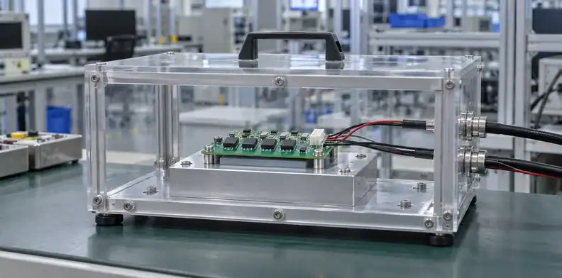
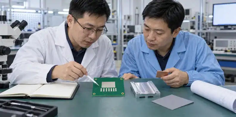
Submit the exact package and a net-annotated local section with the thermal and insulation requirements. This lets the quotation distinguish a conventional via build from an insert-dependent fabrication and assembly proposal.
Include the MOSFET part number and recommended footprint; identify the exposed pad, driver-source and power-source connections. Provide the operating loss envelope, cooler mating temperature and junction design target. Attach the cooler drawing with its electrical reference, mounting features and usable contact area.
For the board itself, send the stackup, layer connections, via treatment and local keepouts. A coin proposal needs its electrical connection and the separate insulating interface. A ceramic proposal needs the material grade, metallization, bonding layers and minimum edge setbacks. Describe the insulation requirement and who supplies the approved verification procedure.
Request separate identification of the offered board process, any specialist insert integration, the assembly steps and the proposed prototype checks. Leave unfamiliar process or test capability for explicit confirmation. A copper-coin drawing or embedded-AlN concept supplied with an inquiry does not establish that QueenEMS offers that exact construction or an accredited isolation test.
For a quotation assessment, send the device datasheet, annotated pad-to-cooler section, loss envelope and mechanical cooler drawing through QueenEMS’s project contact form. Ask the response to identify the feasible board route, unresolved insulation interfaces and any assembly or specialist-process assumptions that affect the quoted scope.
Sources
- Wolfspeed PRD-06752, PCB Layout Techniques for Discrete SiC MOSFETs, Rev. 01, September 2024.
- Kyocera, Aluminum Nitride Packages, Substrates and Submounts.
Written by the QueenEMS Engineering Team
Upload your files today · Free DFM check before production · Ship worldwide
Get your PCB prototypes in as fast as 24 hours. We handle FR4, Rogers, and hybrid boards up to 40 layers in volume production, with advanced builds subject to engineering review — free prototypes for 2–4 layer FR-4 boards, no minimum order.
Just upload your Gerber + BOM — we source every part, assemble, and inspect (AOI + X‑Ray) so you don't have to chase suppliers. Boards ship in as fast as 24 hours.