
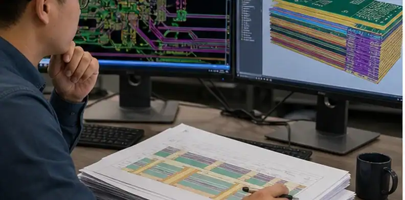
Quick Answer: Decision: high-speed hybrid stackup. Controlled object: electrical construction map connecting critical signals to reference planes, dielectric thickness, material Dk/Df, foil roughness, glass style, and coupon structures. Design-owned boundary: critical signal and plane layers, target impedance, loss budget, return paths, copper profile, weave controls, and validation bandwidth. Supplier discretion: fabricator tuning that stays inside the approved electrical model and returns updated field values before release. Stop rule: critical routing moved to another dielectric, reference plane split, roughness unspecified against a tight loss budget, or nonrepresentative coupon geometry.
The practical question behind high speed hybrid PCB stackup is not whether hybrid construction is possible. The real question is whether the proposed material mix solves the buyer’s performance problem without creating a hidden manufacturing, inspection, lead-time, or repeat-order problem.
Table of Contents
- Start with the layer that creates the requirement
- Separate material savings from build assumptions
- Make impedance and return paths visible
- Control what CAM may change
- Ask for evidence that matches the risk
- Send a quote package that can be compared
- Review copper roughness and glass weave before release
- Lock the production baseline after the first accepted lot
- Separate prototype approval from production release
- Use RFQ wording that protects high-speed electrical intent
Start with the layer that creates the requirement
The first useful step for high speed hybrid PCB stackup is to identify the layer or routing region that actually needs special treatment. In many projects, only RF feeds, long SerDes routes, connector breakouts, antenna sections, or phase-sensitive paths justify the low-loss material.
Once that layer is named, the rest of the stackup becomes easier to discuss. Power planes, mechanical support layers, low-speed control, and shielding may be able to use FR4 or a compatible high-Tg material, but only after the return path and manufacturing balance are reviewed.
Decision signal: The hybrid choice is justified by a named signal or manufacturing requirement, not by a vague preference for premium material.
Separate material savings from build assumptions
| Quote line | What it means | Buyer check |
|---|---|---|
| Material area | How much premium laminate remains | Which layers truly need it? |
| Lamination complexity | Extra process planning or press control | Is it included in the quote? |
| Impedance evidence | TDR or coupon verification | Which nets and layers are tested? |
| Lead time | Material and process queue | What drives the schedule? |
| Repeat order | Ability to rebuild the same stackup | Is the stackup record preserved? |
That is the boundary with older material pages: they help pick a laminate family, while this article helps decide whether the high speed hybrid PCB stackup quote is actually controlled.
Make impedance and return paths visible
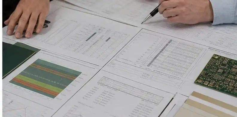
Hybrid stackups can change trace width, spacing, dielectric height, copper roughness, and reference-plane behavior. Those details decide whether the board meets controlled impedance, insertion-loss, skew, or RF launch expectations.
The RFQ should identify the critical nets or structures and the evidence needed for them. A TDR coupon may be right for controlled digital interfaces, while an RF launch or antenna feed may also need layout review, surface finish control, and supplier feedback on manufacturable geometry.
| High-speed concern | Stackup information needed | Evidence to request |
|---|---|---|
| Insertion loss | Dielectric material, copper roughness, and route length | Supplier stackup note or loss-related review |
| Controlled impedance | Layer pair, dielectric height, trace geometry, tolerance | Coupon or TDR plan |
| Skew sensitivity | Glass style and routing layer | Engineering review of material and glass choice |
Test rule: Do not approve a hybrid quote that names impedance targets but does not say how the supplier will verify the relevant layer pair.
Control what CAM may change
A clean RFQ separates allowed supplier proposals from changes that require buyer approval. The fabricator may suggest an equivalent prepreg or thickness adjustment, but material family, critical layer assignment, finished thickness, and evidence requirements should not silently change.
Ask for evidence that matches the risk
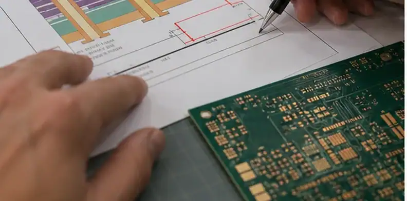
Proof call: The evidence should answer the risk that justified hybrid construction, not fill a folder with generic quality paperwork.
Send a quote package that can be compared
Review copper roughness and glass weave before release
Lock the production baseline after the first accepted lot
Separate prototype approval from production release
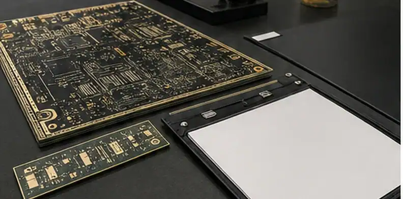
A prototype high-speed hybrid board can pass functional testing while still leaving production questions open. The buyer should separate “the sample works” from “the stackup is approved for repeat production” because the second statement needs controlled material availability, coupon method, copper foil, supplier exceptions, and repeatable evidence.
This is especially important when the first build uses available material, a special engineering review, or a small panel arrangement that may not be used later. A production quote should confirm that the same high speed hybrid PCB stackup assumptions can be repeated at the required quantity and lead time.
Production release: Treat the first accepted lot as evidence for the next order only after the supplier confirms which stackup, material, copper, and test assumptions will remain unchanged.
Use RFQ wording that protects high-speed electrical intent
A high-speed RFQ should identify the electrical reason for the hybrid stackup. Without that reason, the supplier may quote a build that is manufacturable but not equivalent to the loss, skew, or impedance expectation behind the layout.
Practical wording can say: quote the attached high speed hybrid PCB stackup for the listed critical nets and layer pairs. Confirm the proposed low-loss material, FR4 or support material, copper foil type, dielectric thickness, impedance target, coupon method, and any CAM geometry change needed to meet the electrical requirement.
The wording should also separate simulation intent from factory evidence. The designer may have simulated with a nominal Dk and trace width, but the supplier will build with available laminate, prepreg, copper foil, plating, and etch compensation. The quote should say where those manufacturing realities change the numbers.
Purchasing can then compare suppliers by the returned assumptions. One quote may be lower because it omits low-profile copper, uses a weaker evidence package, or treats impedance as best-effort. Another may look higher but include the test evidence needed for release. That is a better comparison than unit price alone.
Electrical rule: The RFQ should preserve the high-speed intent by naming the critical nets, layer pairs, materials, and verification method.
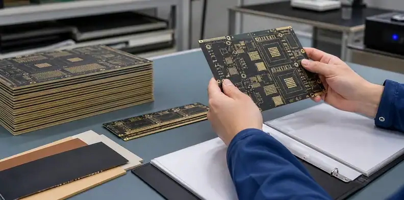
For high-speed programs, the production baseline should also include the routing structures that drove the hybrid choice. List the critical connectors, SerDes lanes, clock paths, memory interfaces, or backplane transitions that must remain tied to the approved layer pair. That prevents a future cost review from moving one critical route to a cheaper layer without realizing why the original construction was selected.
A useful internal note can be short: preserve low-loss material and copper foil on the named high-speed layers unless engineering re-simulates and approves the change. This note gives purchasing a safe boundary when suppliers propose cheaper alternates, and it gives the fabricator a clear reason to ask before changing material or coupon assumptions.
Production record for the high-speed hybrid stackup
Controlled object
Controlled object: electrical construction map connecting critical signals to reference planes, dielectric thickness, material Dk/Df, foil roughness, glass style, and coupon structures.
Failure boundary
Failure boundary: extra insertion loss, skew, return-path discontinuity, impedance drift, resonance, or a coupon that does not represent the routed layer pair.
Design-owned conditions
Design-owned conditions: critical signal and plane layers, target impedance, loss budget, return paths, copper profile, weave controls, and validation bandwidth.
Supplier discretion
Supplier discretion: fabricator tuning that stays inside the approved electrical model and returns updated field values before release.
Required proof
Required proof: field-solver stackup, representative impedance coupon, material and foil record, and test data matched to the actual high-speed layer pairs.
Production stop
Production stop: critical routing moved to another dielectric, reference plane split, roughness unspecified against a tight loss budget, or nonrepresentative coupon geometry.
Repeat-order baseline
Repeat-order baseline: electrical stackup revision, models, material and foil lots, coupon design, measured results, deviations, and production change triggers.
RFQ inputs
RFQ inputs: critical-net list, frequency or edge-rate context, stackup model, target impedances, loss and skew limits, material options, route topology, quantity, and evidence plan.
FAQ
Can the supplier decide the high-speed hybrid stackup?
Discretion for high-speed hybrid stackup: fabricator tuning that stays inside the approved electrical model and returns updated field values before release. Engineering control for high-speed hybrid stackup: critical signal and plane layers, target impedance, loss budget, return paths, copper profile, weave controls, and validation bandwidth.
What stops this high-speed hybrid stackup?
Stop rule for high-speed hybrid stackup: critical routing moved to another dielectric, reference plane split, roughness unspecified against a tight loss budget, or nonrepresentative coupon geometry. Disposition owner for high-speed hybrid stackup: the named engineering approver.
Which proof closes the high-speed hybrid stackup?
Evidence for high-speed hybrid stackup: field-solver stackup, representative impedance coupon, material and foil record, and test data matched to the actual high-speed layer pairs. Revision link for high-speed hybrid stackup: the quoted dataset.
What survives into the next order?
Reorder baseline for high-speed hybrid stackup: electrical stackup revision, models, material and foil lots, coupon design, measured results, deviations, and production change triggers.
For a focused high-speed hybrid stackup, send QueenEMS critical-net list, frequency or edge-rate context, stackup model, target impedances, loss and skew limits, material options, route topology, quantity, and evidence plan. Redline request: high-speed hybrid stackup. Open assumptions: high-speed hybrid stackup. Approver: high-speed hybrid stackup owner.
Written by the QueenEMS Engineering Team
Sources
Upload your files today · Free DFM check before production · Ship worldwide
Get your PCB prototypes in as fast as 24 hours. We handle FR4, Rogers, and Flex up to 60 layers — free prototypes for 2–4 layer boards, no minimum order.
Just upload your Gerber + BOM — we source every part, assemble, and inspect (AOI + X‑Ray) so you don't have to chase suppliers. Boards ship in as fast as 24 hours.