
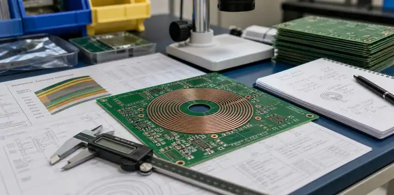
Quick Answer: PCB coil design is ready for fabrication only when the released files lock the spiral geometry, copper weight, layer stack, mask state, finish, and any inspection evidence needed after the build. A PCB supplier can manufacture the released copper pattern, but should not be asked to guess inductance, resistance, coupling, tuning margin, or wireless-power behavior from incomplete Gerbers. For RFQ, send Gerber or ODB++ data, a fabrication drawing, stack-up, coil target notes, panel limits, and a named approval path for coil-area changes.
PCB coil design becomes a sourcing risk when the coil is treated like ordinary routing. The spiral may sit on FR4, flexible material, or a multilayer stack and may serve a sensor, NFC antenna, wireless-power receiver, inductive switch, or tuning structure. The board shop still sees copper that must be etched, plated, masked, finished, inspected, and packed without changing the electrical intent.
This article focuses on the manufacturing handoff. It does not replace electromagnetic simulation, IC vendor design tools, or final product validation.
Table of Contents
- What makes coil copper different from normal routing?
- Which coil dimensions belong in the RFQ package?
- How does copper weight change coil risk?
- When do solder mask and finish need special notes?
- What changes when the coil uses several layers?
- Which CAM questions should pause production?
- What inspection evidence is useful for coil boards?
- How should buyers send coil files to QueenEMS?
What makes coil copper different from normal routing?
A PCB coil is a functional copper structure, so small fabrication changes can affect the finished circuit more than they would on a normal signal trace. Width, gap, corner shape, turn count, via placement, copper thickness, solder mask coverage, and nearby copper all become part of the coil behavior.
Normal routing sometimes allows small supplier-side adjustments during CAM review. A coil is less forgiving because changing a spiral line or gap can shift resistance, inductance, heat rise, or coupling. The fabrication drawing should separate manufacturability questions from electrical design choices.
IC vendor resources for inductive sensing and NFC design usually treat the coil as part of the whole circuit. That design work is necessary, but the procurement handoff still needs a practical manufacturing answer: what exact copper pattern should the board supplier build, and what proof should receiving expect?
Treat the coil area like a controlled feature, similar to an impedance trace, RF launch, current shunt, or antenna keepout. It deserves drawing notes and a CAM review focus.
One useful way to mark the boundary is to place a keepout box or note around the coil in the fabrication drawing. The note can say which copper edits are forbidden, which nearby copper pours may be adjusted for balance, and who approves a change. That small drawing habit prevents a normal CAM cleanup from becoming an unreviewed electrical change.
RFQ signal: The coil is not quote-ready until the geometry is controlled as a manufacturing feature, not merely shown as copper in the Gerber file.
Which coil dimensions belong in the RFQ package?
Freeze the dimensions that define the coil before RFQ: line width, spacing, inner diameter, outer diameter, turn count, corner style, layer assignment, via locations, and target finished copper. The supplier can quote tolerance around a released design, but should not choose geometry that belongs to electrical engineering.
The common mistake is sending Gerbers with no coil notes and assuming the board house will know which features are sensitive. Without notes, a spiral may be treated as dense copper routing rather than a controlled inductor, antenna, or power-transfer feature.
| Coil item to freeze | Why it affects the board | Where to show it |
|---|---|---|
| Trace width and spacing | Sets resistance, etch risk, and current density | Gerber/ODB++ plus drawing |
| Turn count and diameter | Controls magnetic area and layout fit | Layout and mechanical note |
| Finished copper thickness | Changes heat, resistance, and etch profile | Stack-up and RFQ notes |
| Layer location | Sets distance to planes or shields | Stack-up and layer map |
| Via transitions | Add resistance and plating dependence | Drill table and coil note |
| Mask or exposed copper | Controls corrosion, contact, and inspection | Mask data and finish note |
The table is a release-control tool, not a request for the supplier to redesign the coil. When the target inductance, resistance, or tuning range is not final, keep the job in engineering review before pushing it to production quotation.
QueenEMS can check whether the fabrication package is clear enough for quotation, similar to a free PCB DFM check, but the design owner should approve the electrical target and released layout.
Release rule: Any change to coil width, spacing, turns, copper weight, layer, or exposed-copper treatment needs engineering approval.
How does copper weight change coil risk?
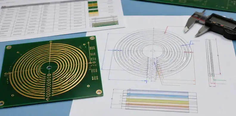
Copper weight changes a PCB coil through resistance, current capacity, heat rise, etching behavior, and cost. Heavier copper can lower DC resistance, but it also makes fine spacing harder to etch and may force wider process assumptions.
For low-current sensing coils, standard copper may be enough when the IC vendor design rules and measured prototype behavior agree. For wireless power, heaters, current-sensing structures, or coils carrying higher current, copper weight becomes both a design and sourcing decision. A 1 oz, 2 oz, or heavier callout changes the line and gap the supplier can hold.
Use the stack-up to state finished copper thickness, not only starting foil when plating contributes to the final conductor. Plated copper, base copper, and etched sidewalls do not behave like an ideal rectangular conductor.
| Copper choice | Manufacturing effect | Buyer action before RFQ |
|---|---|---|
| Standard copper | Easier fine etching and lower cost | Confirm resistance still fits the circuit |
| 2 oz copper | Lower resistance but wider gaps may be needed | Ask whether the coil spacing remains buildable |
| Heavy copper | Better current handling with higher etch risk | Review capability before price comparison |
| Mixed copper layers | Adds stack-up and plating questions | Mark the coil layer and reason clearly |
If the coil is part of a power path, compare it with the broader board current requirement. QueenEMS has separate articles on heavy copper PCB design and PCB copper weight selection. Keep this coil review focused on whether the selected copper weight still supports the released spiral.
Buyer call: Approve copper weight together with minimum line, minimum gap, target resistance, and heat condition.
When do solder mask and finish need special notes?
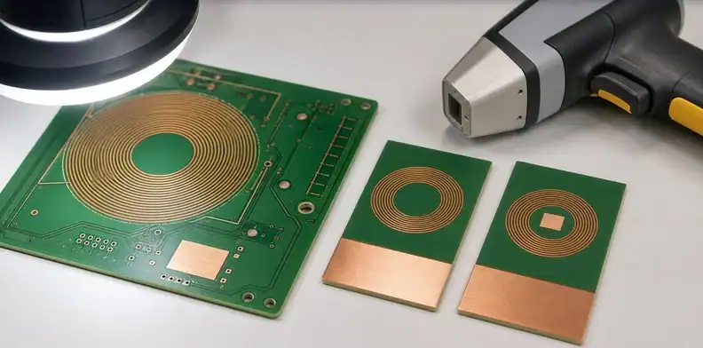
Solder mask and finish need special notes when the coil must remain exposed, contact a spring, accept solder, support probing, avoid corrosion, or maintain a defined distance to a mechanical part. Many internal or protected coils can remain mask-covered; exposed coil copper needs a named function.
Open copper can be intentional for tuning, measurement, contact, or thermal reasons. It can also appear by accident when mask expansion is copied from another feature. The drawing should tell the supplier which case applies.
Surface finish also changes the quote and receiving expectation. ENIG, OSP, immersion silver, HASL, and hard gold do not serve the same function. A coil area touched by a fixture or spring contact should be called out separately from ordinary solder pads.
| Coil surface condition | When it fits | What to specify |
|---|---|---|
| Mask-covered coil | Protected sensing or coupling structure | Mask clearance and no exposed copper |
| Exposed copper segment | Test, tuning, contact, or soldering need | Exact exposed area and finish |
| ENIG on pads only | Stable solderability or probe contact | Pad locations and XRF evidence if needed |
| Hard gold contact area | Repeated mechanical contact | Selective hard-gold area and geometry |
| OSP on simple pads | Cost-sensitive solder-only use | Storage and assembly timing expectation |
For finish-controlled features, the general PCB surface finish thickness requirements are a useful companion. The coil note should still identify the functional area.
Proof rule: Exposed coil copper needs a purpose, a finish, and an inspection expectation.
What changes when the coil uses several layers?
Multi-layer coil designs add via resistance, layer registration, stack-up thickness, dielectric spacing, and hidden geometry that cannot be inspected from one board surface. A stacked coil may be valid electrically, but it needs a clearer fabrication release than a single-layer spiral.
From the PCB supplier’s side, the first questions are practical: which layers are part of the coil, how the layers connect, what copper thickness applies to each layer, and whether the vias are through, blind, buried, or filled. The same layout area may behave differently after a stack-up change.
Via transitions deserve attention. Each via adds conductor length, plating dependence, and a possible current-density point. On a low-current sensing coil this may be minor; on a power-transfer coil it can become a heating or reliability concern.
Layer-to-layer distance also changes behavior. A coil placed over a solid plane, battery shield, metal enclosure, or dense copper pour may not behave like the same spiral in open space. Tie the coil stack to the full product requirement, including the mechanical thickness decision covered in QueenEMS’ PCB board thickness selection article.
Design boundary: The PCB supplier can review layer construction and via manufacturability, but the design owner approves stacked-coil behavior and nearby metal assumptions.
Which CAM questions should pause production?
CAM questions should pause production when the supplier cannot tell which coil geometry is locked, which copper thickness is required, or which process change is allowed. The most common holds are trace/space capability, unclear copper weight, conflicting mask data, undefined finish, and no approval owner for coil-area edits.
These questions are not bad signs. A good CAM hold can prevent a wrong build. Delay starts when the buyer cannot answer quickly or when purchasing approves a geometry change without engineering review.
| CAM question | Why it appears | Best buyer response |
|---|---|---|
| Can trace width or spacing change? | Etch or yield risk | Approve or reject the exact proposal |
| Is the coil exposed or mask-covered? | Mask data and drawing conflict | Confirm the coil-area mask rule |
| Is 2 oz copper required here? | Stack-up and note mismatch | Provide a final copper table |
| Are vias inside the coil locked? | Drill placement affects behavior | Confirm positions or movement limit |
| Do you need resistance measured? | RFQ asks for a value without method | Define pads, temperature, and use |
| Can dummy copper be added nearby? | Panel or plating balance risk | Approve only outside keepout areas |
The broader PCB CAM questions before production workflow is helpful here. For coil boards, no copper-path edit should move ahead without a written response from the design owner.
CAM hold rule: Pause the order when a proposed CAM edit changes the coil path, not only when it changes the board outline or drill file.
What inspection evidence is useful for coil boards?
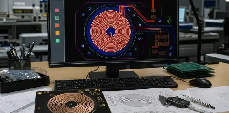
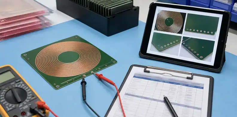
Useful coil-board evidence proves that the manufactured board matches the released feature. Ask for finished width or spacing where measurable, solder mask state, finish coverage, drill/via integrity, board thickness, and clear photos of the coil region. Do not request a long quality package that nobody will review.
For prototypes, a coil-area photo, first-article dimensional check, and confirmation that mask and finish match the drawing may be enough. For production, the file may need lot traceability, continuity data, and targeted dimensional measurements.
Electrical values need careful wording. A board supplier can usually perform continuity or open/short testing, but target inductance, Q factor, coupling efficiency, tuning range, or wireless-power performance may require the customer’s fixture or final assembly.
| Evidence request | Fits this situation | Watch point |
|---|---|---|
| Coil-area photo | Prototype and first build review | Photo is not dimensional proof |
| Trace/space measurement | Fine coils near supplier limits | Define the measurement location |
| Continuity test | Coil path must not be open | Does not prove inductance |
| Resistance spot check | DC resistance is a release concern | Define pads, temperature, and tolerance |
| Solder mask inspection | Covered or exposed copper matters | Compare against the mask data |
| Finish evidence | Exposed pads or contacts are controlled | Match evidence to selected finish |
Tie inspection to receiving use. When receiving will reject exposed copper in the wrong area, put that in the drawing. When engineering only wants photos for prototype learning, state that expectation plainly.
Receiving should also know what not to reject. Slight solder mask shade variation, normal copper color difference under finish, or a photo that does not include every turn may not matter if the controlled evidence is dimensional or electrical. Put the acceptance priority in the purchase record so quality does not escalate cosmetic observations as coil failures.
Acceptance rule: Request evidence that matches the failure mode; continuity, resistance, dimensional checks, photos, and finish records answer different questions.
FAQ
Can a PCB supplier calculate my coil value?
No, the supplier can review and fabricate the released copper geometry, but the design owner should calculate or simulate the coil value and validate it in the product circuit.
Should every coil board include a resistance test?
No, request resistance testing only when DC resistance is part of the acceptance plan. Define pads, temperature, and tolerance before quotation.
Can CAM add copper near a coil for plating balance?
Yes, but only outside the controlled coil keepout and only when engineering confirms the added copper will not affect coupling, tuning, heat, or clearance.
How should buyers send coil files to QueenEMS?
A quote-ready coil package should let the supplier price and review the board without redesigning the coil. Send fabrication data, a controlled drawing, stack-up, material and copper requirements, finish, target electrical notes, inspection expectations, and the approval owner for coil-area changes.
For a clean handoff, include final Gerber or ODB++ data, drill files, layer map, controlled coil drawing note, minimum line and gap, solder mask rule, selective finish areas, target resistance or test points when those values guide review, and any keepout that affects nearby copper or fixtures.
Useful RFQ wording is: “Coil area L1 is controlled. Do not change width, spacing, turn count, via positions, mask opening, or finish without written engineering approval. Please flag any trace/space, copper thickness, or solder mask concern before production.”
Use the QueenEMS contact page to share the final Gerber or ODB++ package, stack-up, coil geometry note, copper weight, mask/finish treatment, target measurement notes, quantity, and inspection request. The review can then concentrate on manufacturability, quote assumptions, and coil-area hold items before release.
Sources
- Texas Instruments, Sensor Design for Inductive Sensing Applications Using LDC
- STMicroelectronics, NFC Inductance Design Tool
Written by the QueenEMS Engineering Team
Upload your files today · Free DFM check before production · Ship worldwide
Get your PCB prototypes in as fast as 24 hours. We handle FR4, Rogers, and hybrid boards up to 40 layers in volume production, with advanced builds subject to engineering review — free prototypes for 2–4 layer FR-4 boards, no minimum order.
Just upload your Gerber + BOM — we source every part, assemble, and inspect (AOI + X‑Ray) so you don't have to chase suppliers. Boards ship in as fast as 24 hours.