

Quick Answer: Your HDI PCB DFM checklist must enforce strict rules to avoid manufacturing rejections: maintain a microvia aspect ratio of ≤1:1, use a minimum annular ring of 15µm, limit stacked microvias to 2 layers, require 100% void-free VIPPO filling, and keep stackup warpage below 0.75%. Skipping any single rule causes immediate no-bid status from fabricators or leads to a 30%+ yield loss during assembly.
Key takeaways:
- Aspect Ratio Limits: A 0.75:1 aspect ratio prevents uneven copper plating and open circuits.
- Stacking Restrictions: Stacking microvias beyond 2 layers severely drops thermomechanical reliability.
- Clearance Needs: Dense HDI boards require strict layer-by-layer IPC-2221 clearance checks.
- Cost Break-Even: Proper layer pairing and documentation shave 2-5 days off engineering hold times.
Table of Contents
- 1. What Is an HDI PCB DFM Checklist and Why Does It Matter?
- 2. How Do You Set Microvia Aspect Ratio for Your HDI PCB DFM Checklist?
- 3. What Annular Ring Rules Should Be in Your HDI Design?
- 4. How Do Stacked vs Staggered Microvia Rules Affect HDI Yield?
- 5. What Trace/Space and Clearance Rules Trigger No-Bid Status?
- 6. How Should You Specify Via-in-Pad (VIPPO) for Reliable HDI Assembly?
- 7. Why Does Stackup Symmetry Belong on Every HDI PCB DFM Checklist?
- 8. What Materials and Dielectric Thickness Rules Apply to HDI Boards?
- 9. How Do You Document Layer Pairs and Drill Files Correctly?
- 10. What HDI DFM Mistakes Cause 30%+ Rework Cost?
You finish routing a dense 0.4mm BGA, send the manufacturing files to fabrication, and immediately get hit with an engineering hold. Overlooked microvia structures, missing layer pair definitions, and broken clearances routinely turn cutting-edge layouts into unmanufacturable nightmares. By using a strict factory-level evaluation process before exporting Gerbers, you guarantee first-pass fabrication success. Utilizing expert HDI PCB fabrication services and running a rigid pre-flight check eliminates these costly redesign loops completely.
1. What Is an HDI PCB DFM Checklist and Why Does It Matter?
An HDI PCB DFM checklist is a mandatory pre-fabrication verification protocol containing 8 to 10 strict physical rules, such as aspect ratio limits (≤1:1) and maximum stacked layers. Implementing this checklist prevents standard multi-layer errors from contaminating microvia architectures, which reduces engineering hold times by 2-5 days. Failing to meet these specific thresholds results in direct no-bid responses from manufacturers.
The Front-End Self-Check List
A frustrated designer on the SierraConnect forum stated: “One of the most frequent causes of board delays isn’t routing complexity. It’s preventable DFM issues discovered after files reach fabrication. These problems aren’t limited to complex HDI boards.” To prevent these delays, you must run this 8-point self-check before submitting files:
- Verify microvia aspect ratios are ≤1:1.
- Check that annular rings are ≥15µm for volume production.
- Confirm stacked microvias do not exceed 2 continuous layers.
- Verify VIPPO structures specify 100% epoxy filling.
- Confirm stackup warpage limits are set to <0.75%.
- Check that minimum trace/space is ≥30µm (1.2mil).
- Ensure impedance specs are explicitly mapped to specific trace widths.
- Verify drill files clearly define specific start and stop layers.
The QueenEMS Engineering Perspective
We frequently see clean layouts fail at the documentation stage because designers skip basic output checks.
- The Problem: A startup submitted a complex ODB++ package but forgot to include a formal stackup drawing and clear layer-pair definitions for their blind vias.
- Our Solution: We paused the job, generated a missing-data report, and established an 8-point frontend checklist for their engineering team.
- The Result: By fixing their export protocol, we reduced their typical pre-production engineering hold time from 4 days down to just 4 hours, accelerating their market launch.
Bottom line: Documenting your stackup, layer pairs, and impedance specs in fabrication notes prevents 80% of engineering questions and shaves days off your lead time.
2. How Do You Set Microvia Aspect Ratio for Your HDI PCB DFM Checklist?
Microvia aspect ratio must not exceed 1:1 per the IPC-T-50M standard, with 0.75:1 being the preferred target for high-yield volume production. Exceeding this physical limit causes uneven copper plating inside the hole, which is the root cause of 80% of microvia failures during thermal cycling. Proper microvia design optimization directly translates to reliable signal continuity.
Sizing for Reliability
A common question on SierraConnect asks: “How should I size my microvias? Their reliability is sensitive to design choices like aspect ratio, layer pairing, and copper plating.”
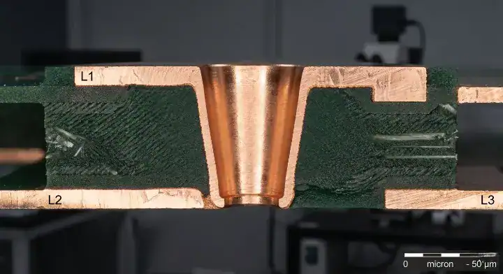
A microvia is a laser-drilled hole with a finished diameter of ≤150µm (6mil) that connects adjacent layers. To size them correctly, define your stackup first. Find the dielectric thickness, then use the 1:1 aspect ratio rule to calculate your minimum hole size. Finally, apply your manufacturer’s annular ring tolerance to dictate the capture pad size.
Preventing Thermal Expansion Failures
Because different materials expand at different rates during reflow, severe CTE (Coefficient of Thermal Expansion) mismatch occurs. The epoxy resin expands at ~200ppm/°C while copper expands at just 16ppm/°C, resulting in massive Z-axis stress. A high aspect ratio via will fracture at the target pad interface under this stress. Sierra Circuits recommends utilizing D-coupon testing; if via chain resistance changes by more than 5%, the structure fails IPC qualification.
Bottom line: If your microvia aspect ratio exceeds 1:1, expect a no-bid status from any reputable HDI fabricator because the plating chemistry cannot reach the bottom of the hole.
3. What Annular Ring Rules Should Be in Your HDI Design?
HDI annular ring requirements mandate a minimum of 25µm (1mil) per IPC-2226 for standard designs, but manufacturers strongly recommend a 15µm absolute minimum after processing to survive volume production. An insufficient annular ring leads to drill breakout, where the laser slightly misses the pad center, completely severing the electrical connection. Using a reliable PCB annular ring formula guide prevents these costly open circuits.
Managing Laser Drill Accuracy
Standard mechanical drills suffer from drill wander, but laser drills have high precision. The typical laser drill tolerance is ±5µm. For a 0.3mm pitch BGA, you generally need a 75-100µm drill hole paired with a 150µm capture pad to maintain a safe margin. If you shrink the pad to 120µm to force traces through tight spaces, a 5µm alignment shift instantly risks a breakout failure.
Establishing Teardrops
To add mechanical strength to your annular rings, you should aggressively use teardrops at every trace-to-pad junction. A teardrop adds extra copper where the thin trace meets the via pad, which acts as a physical buffer if the laser drill wanders slightly off-center. This simple CAD setting dramatically increases your overall board yield.
Bottom line: Never set your CAD tools to allow a 0µm annular ring; always design with a 25µm target to guarantee that microscopic misalignments do not destroy your board.
4. How Do Stacked vs Staggered Microvia Rules Affect HDI Yield?
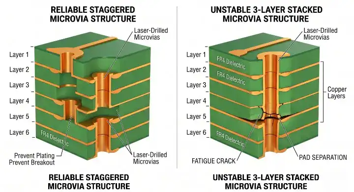
Stacked microvias must never exceed 2 continuous layers because thermal stress causes a severe reliability drop at 3 layers, reducing overall HDI yield by 20-30%. According to an IPC 2019 reliability warning, staggering your microvias with an offset of ≥100µm distributes the Z-axis expansion stress safely across the FR4 material. Staggered structures cost slightly less because they do not require complex planarization between every single layer.
The Stacking Danger Zone
Engineers often face pushback from factories, as noted in this forum complaint: “I want to use stacked microvias for max density on my 0.4mm BGA. Manufacturer is pushing back—why?”
The factory pushes back because stacked vias beyond 2 layers represent a massive liability. When you stack vias directly on top of each other, the copper interfaces experience compounding thermal expansion stress during assembly reflow. Furthermore, you should never stack a microvia directly on top of a buried mechanical via, as the resin shrinkage will inevitably pull the microvia apart.
The QueenEMS Engineering Perspective
Pushing the limits of stacked vias is the fastest way to ruin a production run.
- The Problem: A customer submitted a 0.4mm BGA board featuring a 3-layer stacked microvia structure with a dangerous 1.3:1 aspect ratio.
- Our Solution: We conducted a DFM review and convinced the client to change the layout to staggered microvias with an offset, reducing the aspect ratio to 0.85:1 and increasing the annular ring to 15µm.
- The Result: The first-pass assembly yield skyrocketed from an abysmal 68% up to 94%, completely eliminating the field failures they previously experienced.
Bottom line: Stacked microvias beyond 2 layers is not a clever density optimization—it is a severe reliability liability. Use staggered structures whenever board space permits.
5. What Trace/Space and Clearance Rules Trigger No-Bid Status?

Trace and space clearances below 30µm (1.2mil) immediately trigger a no-bid status from most standard HDI fabricators because standard etching processes cannot resolve lines that thin. HDI dense routing inherently forces traces close together, meaning you must enforce strict layer-by-layer Design Rule Checks (DRC) to ensure you do not violate IPC-2221 voltage clearance standards.
High Voltage Clearances in HDI
An engineer on SierraConnect asked: “What is the ideal component clearance for an HDI board operating at 150V?”
According to the IPC-2221 clearance table, a 50V signal on an internal coated layer (B1) requires a 0.025mm gap. However, stepping up to 150V requires a massive 0.4mm gap internally, and a 0.8mm gap for external uncoated layers (B4). You cannot shrink these gaps just because you are using HDI tech; physics still applies, and high voltage will arc across inadequate spaces.
Solder Mask Dams
For ultra-fine 0.4mm pitch BGAs, you must maintain a solder mask dam of at least 15µm between adjacent surface pads. If the clearance is too tight and the manufacturer cannot print the dam, solder paste will bridge across the pads during reflow, resulting in massive short circuits.
| Design Parameter | Standard PCB Tolerance | HDI PCB Tolerance |
|---|---|---|
| Min Trace/Space | 100µm / 100µm | 30µm / 30µm |
| Aspect Ratio Max | 10:1 (Through-hole) | 1:1 (Microvia) |
| Min Annular Ring | 125µm (5mil) | 25µm (1mil) |
| Stackup Warpage | ±1.0% | <0.75% |
Analysis Guide: Choose standard tolerances if your board area allows for wider routing. Switch to the strict HDI tolerances only when your component pitch falls below 0.65mm.
Bottom line: Never apply low-voltage digital spacing rules to high-voltage analog traces inside an HDI board; strict DRC verification is mandatory to prevent arcing and bridging.
6. How Should You Specify Via-in-Pad (VIPPO) for Reliable HDI Assembly?
Via-in-Pad Plated Over (VIPPO) must be explicitly specified with 100% void-free copper/epoxy filling and planarization to guarantee reliable HDI assembly. VIPPO is a technique where the microvia is placed directly inside the surface mount pad, saving immense board space. However, if the via is not completely filled, it causes a 30-40% drop in assembly yield due to solder wicking.
The Solder Wicking Threat
A desperate engineer posted: “Can’t I plug via-in-pad with solder resist for HDI? My board has BGA with via-in-pad and getting solder voiding issues during assembly.”
No, you absolutely cannot use standard solder mask plugging for VIPPO. Because the via sits directly under the component, an unplugged or poorly plugged hole acts like a straw. During the reflow oven cycle, capillary action sucks the liquid solder paste down into the via hole. This starves the surface pad of solder, resulting in a weak, open, or highly resistive joint.
Fabrication Requirements
You must require your fabricator to fill the via with specialized conductive or non-conductive epoxy, cure it, grind the surface completely flat (planarization), and then plate copper over the top. The filled flat tolerance must be within ±5µm. Always demand an X-ray verification check prior to final BGA assembly to ensure zero internal voids.
Bottom line: Specify VIPPO with 100% epoxy fill and planarization in your fab notes; skipping this step to save money guarantees catastrophic solder joint failures at assembly.
7. Why Does Stackup Symmetry Belong on Every HDI PCB DFM Checklist?
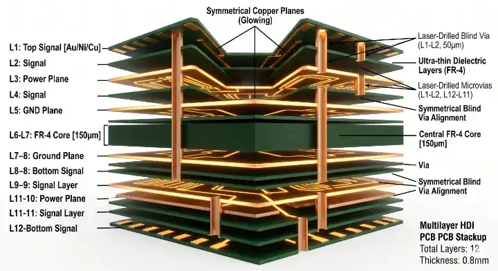
Stackup symmetry belongs on every HDI checklist because asymmetrical copper distribution causes severe bowing and twisting during sequential lamination, pushing stackup warpage beyond the acceptable <0.75% limit defined by IPC-6016. A warped board cannot sit flat inside the SMT pick-and-place machine, resulting in misaligned fine-pitch components. Reviewing PCB stackup design best practices is essential for maintaining mechanical stability.
The Mirror Principle
A symmetrical stackup requires mirrored copper weight and like-layer pairing radiating outward from the precise center core of the board. If Layer 2 utilizes 2oz copper for power delivery, Layer N-1 (the opposite side) must also feature a similar 2oz copper density.
Sequential Lamination Risks
Sequential lamination is the process of pressing the board multiple times to create complex blind and buried via structures. Because HDI boards undergo 2 to 4 press cycles at extremely high temperatures, any asymmetry in the dielectric thickness or copper distribution generates massive internal stress. When the board cools, this stress forces the FR4 to curve like a potato chip, rendering it totally useless for assembly.
Bottom line: Always balance your copper planes and dielectric thicknesses symmetrically across the center axis; an asymmetrical HDI board will warp permanently during the lamination press.
8. What Materials and Dielectric Thickness Rules Apply to HDI Boards?
HDI boards require advanced materials rated under IPC-4104 that can survive multiple sequential lamination cycles without severe resin degradation. Standard FR-4 degrades quickly after two pressings, meaning you must specify high-Tg (Glass Transition Temperature >170°C) materials. Dielectric thickness rules dictate that your prepreg layers must be thin enough (typically 2-4mils) to allow laser drills to maintain the critical 1:1 aspect ratio.
Material Movement and Registration
When dealing with lines and spaces as small as 40µm, material movement becomes a critical DFM parameter. During the pressing cycle, resin flows and fiberglass weaves shift. Your manufacturer must use materials with highly predictable dimensional stability to ensure that the laser drills actually hit the microscopic copper pads hidden on the internal layers.
Laser Drill Penetration limits
Laser drills utilize specific wavelengths (UV or CO2) to vaporize resin and glass. They struggle to penetrate thick layers cleanly. If you specify a dielectric thickness of 6mils or higher between layers, the laser must burn longer and wider, creating a tapered, cone-shaped via that violates aspect ratio rules and ruins plating reliability.
Bottom line: Specify high-Tg, dimensionally stable materials and keep your HDI dielectric thicknesses between 2mil and 4mil to ensure clean laser drilling and reliable registration.
9. How Do You Document Layer Pairs and Drill Files Correctly?
Documenting layer pairs and drill files correctly eliminates the confusion that causes 2-5 day delays during the initial CAM engineering review. HDI designs utilize complex sub-laminations involving blind vias (e.g., L1-L2) and buried vias (e.g., L2-L7). If your NC Drill files do not explicitly declare which layers every specific via spans, the factory cannot program their laser drills.
The Ambiguity Trap
Do not rely on software autorouters to generate clean fabrication notes. You must manually generate a text-based drill table on your fabrication drawing. This table must categorize every drill tool by size, specify whether it is plated or non-plated, and most importantly, explicitly list the exact start and stop layers (e.g., “0.1mm Laser Drill, L1 to L3”).
Impedance and Type Declaration
Your fabrication drawing must explicitly state the intended IPC-2226 Type (e.g., “Build to IPC-2226 Type II”). Additionally, clearly map your controlled impedance requirements. Do not just write “50 ohm impedance required.” Specify exactly which trace width on which specific layer targets that 50-ohm value, allowing the factory to tweak the trace slightly to hit your electrical goals.
Bottom line: Never send ambiguous drill files to an HDI fabricator; provide a rigid, explicit drill table that maps every via span to its correct layer pair.
10. What HDI DFM Mistakes Cause 30%+ Rework Cost?
HDI DFM mistakes cause 30%+ rework costs when designers implement false HDI needs, utilize 90° trace corners, or fail to leave center-to-center microvia spacing of ≥50µm. Because sequential lamination and laser drilling are entirely irreversible processes, repairing a failed HDI board is nearly impossible. A single unfillable via under a BGA or a broken ground plane forces a complete scrap of the entire production batch.
Eliminating False HDI Needs
Many designs that appear to require microvias actually suffer from poor basic layout practices. A “false HDI need” occurs when a designer creates artificial congestion. For example, failing to use shared ground vias for bypass capacitors eats up routing channels. By cleaning up these basic DFM mistakes, you can often revert an expensive HDI design back to a much cheaper standard multi-layer build.
| BGA Pitch | Min Via Strategy | Typical Pad Size | Typical Drill Size |
|---|---|---|---|
| 1.0mm | Standard Through-Hole | 24mil | 12mil |
| 0.8mm | Dog-bone Fanout | 20mil | 10mil |
| 0.65mm | Sub-lamination Vias | 16mil | 8mil |
| 0.5mm | VIPPO / Microvia | 10mil | 5mil (Laser) |
| 0.4mm | 2-2-2 Stackup HDI | 9mil | 4mil (Laser) |
Analysis Guide: Match your via strategy strictly to your component pitch. Avoid using expensive 4mil laser drills if your tightest component is a 0.8mm BGA.
The QueenEMS Engineering Perspective
We frequently catch expensive over-engineering mistakes before fabrication begins.
- The Problem: A client submitted a design using 3mil traces for low-current digital signals, forcing the board into an expensive HDI pricing tier despite having no tight BGAs.
- Our Solution: We ran a DFM check and realized they had plenty of physical board space. We globally expanded their trace/space rules to a standard 4mil/4mil.
- The Result: The client avoided the HDI fabrication process entirely, saving 30% on bare board costs and shaving a week off their delivery schedule without impacting performance.
Bottom line: Do not utilize HDI tolerances arbitrarily; only trigger tight microvia and trace rules when component physical constraints absolutely demand it.
Conclusion
Executing a flawless high-density design requires far more than just connecting nets in your CAD software. By enforcing strict rules—maintaining a 1:1 aspect ratio, requiring 100% filled VIPPO, limiting stacked microvias, and ensuring perfect stackup symmetry—you protect your project from catastrophic manufacturing failures. An airtight HDI PCB DFM checklist acts as your final defense against no-bid rejections and massive rework costs.
QueenEMS specializes in transforming complex, high-density layouts into highly reliable physical products. If you are uncertain about your microvia sizing or stackup architecture, contact our DFM engineering team today. We provide comprehensive front-end engineering reviews to ensure your board moves flawlessly from digital design to physical reality.
Written by the QueenEMS Engineering Team
FAQs
Can I stack microvias across 4 layers to save space? No, stacking microvias across more than 2 layers causes a massive drop in thermomechanical reliability. The compounded stress during reflow will fracture the copper joints. Always use staggered microvias with an offset of at least 100µm for deeper layer transitions.
What happens if I don’t fill via-in-pad structures with epoxy? If you do not fill VIPPO structures, capillary action will suck the liquid solder paste down the via hole during assembly reflow. This starves the surface component pad, resulting in a weak or completely open electrical connection, causing severe yield loss.
How do I calculate the minimum microvia hole size? Determine your target dielectric thickness first, then apply the 1:1 aspect ratio rule. If your dielectric thickness is 4mils, your absolute minimum laser-drilled hole size must be 4mils. Attempting to drill a 3mil hole through a 4mil dielectric causes plating failures.
Does an asymmetrical HDI stackup really cause warpage? Yes, an asymmetrical stackup guarantees severe warpage during the sequential lamination process. Because HDI boards undergo multiple high-heat press cycles, unbalanced copper weight or uneven dielectric layers will cause the board to bow, rendering it un-assemblable.
Why did my manufacturer reject my 30µm trace design? Your manufacturer rejected the 30µm design because standard etching processes cannot reliably resolve lines smaller than 75µm without causing shorts or opens. You must partner with a specialized HDI facility equipped with advanced laser direct imaging (LDI) to handle 30µm features.
Upload your files today · Free DFM check before production · Ship worldwide
Get your PCB prototypes in as fast as 24 hours. We handle FR4, Rogers, and Flex up to 60 layers — free prototypes for 2–4 layer boards, no minimum order.
Just upload your Gerber + BOM — we source every part, assemble, and inspect (AOI + X‑Ray) so you don't have to chase suppliers. Boards ship in as fast as 24 hours.