
Quick Answer: A gerber file is a standard 2D vector graphic format that provides PCB manufacturers with exact fabrication instructions. A complete production package requires a minimum of 8 separate files for a standard 2-layer board, dictating copper routing, drill coordinates, and solder mask placement with sub-mil precision. Key takeaways:
- Format consistency prevents 2-10mm drill offsets.
- Standard packages need 8 files for 2-layer designs.
- Missing outlines cause 35% of all CAM holds.
- Newer X2 formats reduce setup time by up to 50%.
Table of Contents
- What Is a Gerber File and Why Does It Matter for PCB Manufacturing?
- What Information Do These Fabrication Documents Contain?
- Which Format Should You Use: RS-274X vs. Gerber X2?
- What Files Must Be Included in a Complete PCB Data Package?
- How Do You Generate a Gerber File From Popular CAD Software?
- How Should You Verify Your Exported Layers Before Production?
- What Are the Most Common Gerber File Mistakes That Delay Production?
- How Do PCB Manufacturers Use Layout Data on the Production Floor?
- Gerber vs ODB++ vs IPC-2581: Which PCB Data Format Is Best?
- How Can You Prevent Format Errors and Speed Up Your PCB Order?
A gerber file is the definitive digital blueprint that tells a fabrication facility exactly how to build your circuit board. You finish routing a complex layout, export the manufacturing data, and send it off, only to receive an urgent engineering hold 12 hours later. Manufacturing delays occur because of missing drill coordinates, mismatched units, or ambiguous outline boundaries, which directly waste your time and budget. Generating a perfect data package makes sure your design moves straight to the imaging department without costly interruptions. If you are submitting data for rapid PCB prototyping, configuring your export settings correctly is the single most critical step in the entire hardware development cycle.
What Is a Gerber File and Why Does It Matter for PCB Manufacturing?
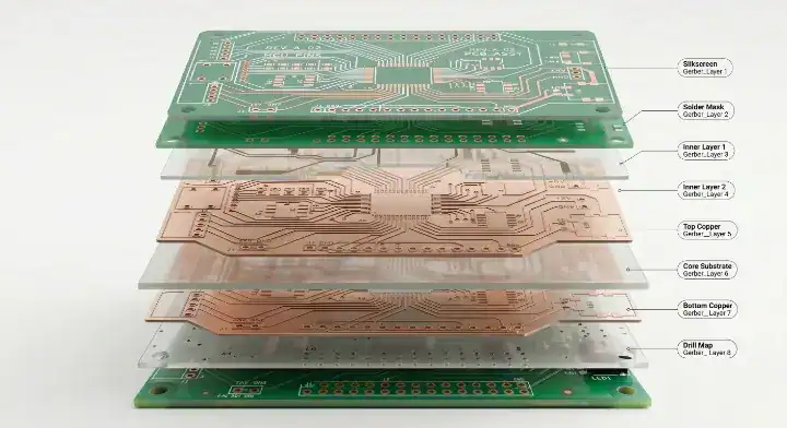
A gerber file is a 2D ASCII text vector file that controls the photoplotters and Laser Direct Imaging (LDI) machines used to create printed circuit boards. According to Ucamco, the official maintainer of the standard, this format is universally supported by all PCB design systems and CAM software worldwide. Each functional layer of your physical board requires one independent document to guide the etching and printing machinery.
The Evolution of Fabrication Formats
Originally designed to drive physical light shutters, this format now drives high-speed digital imaging equipment. The vector data defines the exact geometry of every pad, trace, and via.
Let us look at the details:
- Top and bottom copper routes for electrical connections.
- Solder mask clearances to expose component pads.
- Silkscreen reference designators for assembly mapping.
Key Takeaway: Bottom line: Always provide a dedicated vector text document for every physical material layer of your circuit board.
| Format Element | Function | Industry Standard |
|---|---|---|
| Vector Data | Defines shapes | RS-274X |
| ASCII Text | Human readable | Yes |
| Layer Mapping | 1 file per layer | Mandatory |
| Vector text allows CAM systems to precisely recreate your layout on copper without resolution degradation. |
What Information Do These Fabrication Documents Contain?
Every gerber file contains four specific data structures: configuration parameters, aperture definitions, XY coordinate locations, and flash commands. These instructions tell the manufacturing equipment exactly where to place copper features with an accuracy of 0.001 inches. Missing any of these data blocks causes the entire layer to render incorrectly.
What Is the Anatomy of the Vector Data?
The code reads like a highly specific set of plotting instructions. The aperture definition acts as a digital stencil, while the coordinate data tells the machine where to apply that stencil.
The reality is simple:
- Format parameters define units and coordinate precision.
- Tool definitions establish precise trace widths.
- D-codes control the physical machine movements.
Key Takeaway: Bottom line: Never modify the generated text code manually, because syntax errors will corrupt the entire production run.
| Data Block | Purpose | Example Code |
|---|---|---|
| Header | Unit definition | %MOIN*% (Inches) |
| Aperture | Shape and size | %ADD10C,0.010*% |
| Coordinates | Location mapping | X1500Y2000D02* |
| The text-based nature of this data allows engineers to quickly troubleshoot rendering errors using standard text editors. |

Which Format Should You Use: RS-274X vs. Gerber X2?
RS-274X is the standard gerber file format that embeds aperture definitions directly within the text, while the newer Gerber X2 format adds intelligent metadata attributes. Upgrading to X2 reduces CAM engineering setup time by 30-50% because the software automatically identifies whether a layer is top copper or bottom solder mask. Most modern fabrication plants accept both versions natively.
Comparing Legacy and Modern Exports
The older RS-274D version required a separate aperture list, which frequently caused missing tool errors. The Extended X-version fixed this by self-containing the geometry, but left layer identification up to the engineer.
Here is what you need to know:
- RS-274X is universally accepted by 100% of factories.
- Gerber X2 embeds stackup sequence information.
- X2 attributes prevent negative polarity confusion.
Key Takeaway: Bottom line: Export your designs using the X2 format to eliminate manual layer assignment delays during CAM import.
| Feature | RS-274X | Gerber X2 |
|---|---|---|
| Embedded Apertures | Yes | Yes |
| Layer Attributes | No | Yes |
| CAM Setup Speed | Standard | 30-50% Faster |
| The addition of metadata attributes in X2 prevents costly layer misinterpretations before tooling begins. |
What Files Must Be Included in a Complete PCB Data Package?
A standard 2-layer printed circuit board requires exactly 8 specific gerber file exports to begin manufacturing. These include the top and bottom copper (.GTL, .GBL), top and bottom solder mask (.GTS, .GBS), top and bottom silkscreen (.GTO, .GBO), board outline (.GKO), and the Excellon drill file (.DRL). Adding quick turn PCB assembly requires an additional pick-and-place coordinate document.
What Is the Mandatory Export Checklist?
Many designers submit incomplete archives, causing immediate production holds. The board outline must always be a separate, closed-path layout, which means it cannot be mixed with mechanical dimensions or title blocks.
Consider this standard checklist:
- Copper layers for active electrical routing.
- Solder mask files to define exposed soldering pads.
- Silkscreen graphics for component designators.
Key Takeaway: Bottom line: Always generate a dedicated, single-path outline file to prevent the factory from routing your board to the wrong dimensions.
| Layer Type | File Extension | Necessity |
|---|---|---|
| Top Copper | .GTL | Required |
| Bottom Mask | .GBS | Required |
| Outline | .GKO / .GM1 | Required |
| Separating the board profile from mechanical notes allows automated routers to extract the exact milling path. |
How Do You Generate a Gerber File From Popular CAD Software?
Generating a gerber file requires setting matching coordinate precision across all layers, typically using a 2:5 or 4:6 decimal format. When exporting from tools like KiCad or Fusion 360, mixing imperial and metric units between the copper data and drill data causes the holes to shift 2-10mm off-center. Consistent export parameters are strictly required for proper alignment.
Preventing Drill Offset Errors
A common issue on engineering forums involves drill coordinates misaligning with copper pads after exporting from free software. This happens because the drill file uses a default 3:3 precision while the copper traces use 4:6, resulting in a scale mismatch during CAM processing.
To solve this alignment issue:
- Set all outputs to millimeters or inches strictly.
- Use identical integer and decimal grid settings.
- Generate Excellon drills separately from routing data.
Key Takeaway: Bottom line: Match the coordinate precision and measurement units across every single export window in your CAD software.
| Software | Export Menu | Recommended Precision |
|---|---|---|
| KiCad | File > Plot | 4:6 Metric |
| Altium | Fabrication Outputs | 2:5 Imperial |
| Fusion 360 | CAM Processor | 2:5 Imperial |
| Forcing unit consistency directly prevents the most common cause of drill breakout and scrapped panels. |
How Should You Verify Your Exported Layers Before Production?
You must load your newly generated gerber file package into a third-party viewing tool to verify layer registration and scale. Overlaying the Excellon drill data on top of the copper layers visually confirms that your vias sit perfectly within their designated pads. Taking 5 minutes to run this check catches over 80% of formatting mistakes before manufacturing begins.
How Does the Visual Validation Process Work?
Do not rely solely on your layout software’s native view. Use an independent tool like gerbv or ViewMate to render the raw ASCII data exactly as the factory equipment will read it.
Follow this verification sequence:
- Import all exported layers simultaneously.
- Assign contrasting colors to copper and drill geometries.
- Verify that solder mask openings match physical pad sizes.
Key Takeaway: Bottom line: Always use an independent, third-party viewer to inspect your manufacturing outputs before sending them to a supplier.
| Verification Step | Target Issue | Third-Party Tool |
|---|---|---|
| Drill Overlay | Offset / Scale mismatch | gerbv |
| Mask Check | Missing pad clearances | ViewMate |
| Outline Test | Open routing boundaries | KiCad Viewer |
| Using a separate viewing application isolates design software bugs from the actual manufacturing machine code. |

What Are the Most Common Gerber File Mistakes That Delay Production?
About 15-20% of first-time submissions trigger engineering queries due to gerber file formatting errors. In our CAM department, we process over 300 unique packages every month, finding that missing board outlines cause 35% of delays, inverted solder masks cause 25%, and mismatched drill units cause 20%. Detecting these via a free DFM review saves customers $200-$500 per re-spin and 3-5 days of lost time.
Fixing Empty Masks and Missing Drills
When a manufacturer reports an “empty soldermask” despite your viewer showing data, the polarity is usually set to positive instead of negative. Also, drill coordinates must be exported in a dedicated Excellon format; they cannot be embedded within the copper routing text.
Pay attention to these frequent failures:
- Plated (PTH) and non-plated (NPTH) holes are mixed into one document.
- Solder mask layers use positive polarity rendering.
- Mechanical dimensions intersect the milling boundary.
Key Takeaway: Bottom line: Separate your plated and non-plated drills into two distinct Excellon documents to prevent electroplating errors.
| Common Error | CAM Frequency | Production Impact |
|---|---|---|
| Missing Outline | 35% | Fabrication halted |
| Inverted Mask | 25% | Completely covered pads |
| Mixed Units | 20% | 2-10mm drill offset |
| Implementing a strict pre-submission checklist reduces these specific CAM queries from 30% down to 15%. |
How Do PCB Manufacturers Use Layout Data on the Production Floor?
A manufacturer imports your gerber file directly into specialized Computer-Aided Manufacturing (CAM) software to generate tooling instructions. This process applies etch compensation, which enlarges your copper traces by 0.5 to 1 mil to account for chemical etching shrinkage. The finalized data then drives the LDI machines to expose the dry film photoresist cleanly.
The Factory Processing Sequence
The raw data you provide is never printed directly onto the board. Process engineers modify the shapes to optimize the yield, making slight adjustments to via pad sizes to meet the required PCB via current capacity guide standards.
The production sequence operates like this:
- CAM engineers import and align all text files.
- DFM software checks for minimum 3-mil spacing.
- Algorithms apply etch compensation to specific traces.
Key Takeaway: Bottom line: Design your traces with enough clearance to allow the factory room to apply necessary etch compensation.
| Factory Step | Data Manipulation | Goal |
|---|---|---|
| CAM Import | Layer alignment | Registration |
| DFM Check | Spacing verification | Prevent shorts |
| Etch Comp | Enlarging traces | Counteract acid |
| Understanding that factories slightly alter your vector data helps you design safer clearances. |
Gerber vs ODB++ vs IPC-2581: Which PCB Data Format Is Best?
The standard gerber file format requires 8 to 20 separate documents, whereas IPC-2581 and ODB++ compile all manufacturing data into a single intelligent archive. According to IPC, the vendor-neutral IPC-2581 XML format is the next-generation replacement for multi-file systems. EE Times reports that complex High-Density Interconnect (HDI) boards heavily benefit from these newer formats because they embed rigid material stackup specifications.
Transitioning to Intelligent Data
Traditional vectors lack component intelligence, requiring separate Bill of Materials (BOM) and pick-and-place lists. ODB++ packages the schematic netlist, layout geometry, and component footprint data together, which eliminates ambiguity during the assembly phase.
Consider these formatting distinctions:
- RS-274X delivers purely graphical two-dimensional shapes.
- ODB++ uses a hierarchical folder structure for files.
- IPC-2581 utilizes a single open-source XML standard.
Key Takeaway: Bottom line: Stick to RS-274X for standard 2-4 layer boards, but transition to ODB++ or IPC-2581 for complex HDI and impedance-controlled designs.
| Format | Structure Type | Best Application |
|---|---|---|
| RS-274X | Multiple text files | Standard 2-4 layer |
| ODB++ | Folder hierarchy | Complex assembly |
| IPC-2581 | Single XML | Advanced HDI |
| Intelligent data structures directly reduce the back-and-forth communication required to clarify stackup materials. |
How Can You Prevent Format Errors and Speed Up Your PCB Order?
You can prevent gerber file errors by running strict Design Rule Checks (DRC) and supplying a detailed README document with your submission. We recently processed a 6-layer rigid-flex board where the customer used outdated RS-274D formats for inner layers and a 2:4 precision setting for 0.15mm microvias. Our CAM review caught the annotations crossing the board outline, saving the client $3,200 in scrapped materials and a 2-week delay.
Best Practices for Clean Submissions
Providing clear instructions accelerates the tooling phase. Taking proactive steps also supports your NRE cost reduction strategies by avoiding administrative engineering fees.
The strategy for a fast turnaround involves:
- Zipping all required layers into a single folder.
- Including a README with stackup thickness limits.
- Running a final automated DRC before exporting.
Key Takeaway: Bottom line: Always package your verified vector documents with a detailed text file defining the board material, thickness, and finish.
| Prevention Method | Action Required | Resulting Benefit |
|---|---|---|
| DRC Pass | Fix spacing violations | Zero short circuits |
| README File | List stackup specs | Faster CAM setup |
| Zip Archive | Group all extensions | No missing layers |
| A well-documented submission archive bypasses the standard engineering query queue, resulting in faster manufacturing. |
Generating a flawless gerber file package makes sure that your circuit board transitions from software to the physical production floor without costly delays. By understanding the core differences between RS-274X and newer intelligent formats, maintaining strict coordinate precision, and visually verifying your Excellon drills, you eliminate the alignment errors that plague unverified submissions. Our CAM engineers routinely catch inverted mask polarities and missing outlines before they hit the etching line, protecting your project budget. If you are ready to manufacture your next prototype with zero formatting headaches, contact us today for a detailed design review and immediate production.
FAQ
Can I send my PCB design file directly to a manufacturer without Gerber files? No. Most manufacturers require RS-274X or X2 formats because their CAM systems cannot directly interpret native CAD files from tools like KiCad or Altium. You must export these universal text documents before submitting for fabrication.
How many Gerber files do I need for a standard 2-layer PCB? 8 files are strictly required. You need top and bottom copper, top and bottom solder mask, top and bottom silkscreen, a continuous board outline, and an Excellon drill file to start fabrication.
What is the difference between RS-274X and Gerber X2? RS-274X embeds standard aperture shapes, while Gerber X2 adds intelligent attribute tags. The X2 version explicitly labels each layer’s function, reducing CAM setup time by up to 50% by eliminating identification guesswork.
What’s the best free Gerber viewer to check my files? 2 specific tools dominate the free market: gerbv for open-source Linux/Windows users, and ViewMate for Windows environments. These independent programs reliably render your raw ASCII data to reveal hidden scaling or alignment issues.
How do I know if my Gerber files are ready for manufacturing? Yes, visual confirmation is your final proof. When you overlay the copper, outline, and drill layers in a third-party viewer and see perfect via alignment with a closed routing path, your package is ready for a professional DFM review.
Upload your files today · Free DFM check before production · Ship worldwide
Get your PCB prototypes in as fast as 24 hours. We handle FR4, Rogers, and Flex up to 60 layers — free prototypes for 2–4 layer boards, no minimum order.
Just upload your Gerber + BOM — we source every part, assemble, and inspect (AOI + X‑Ray) so you don't have to chase suppliers. Boards ship in as fast as 24 hours.