
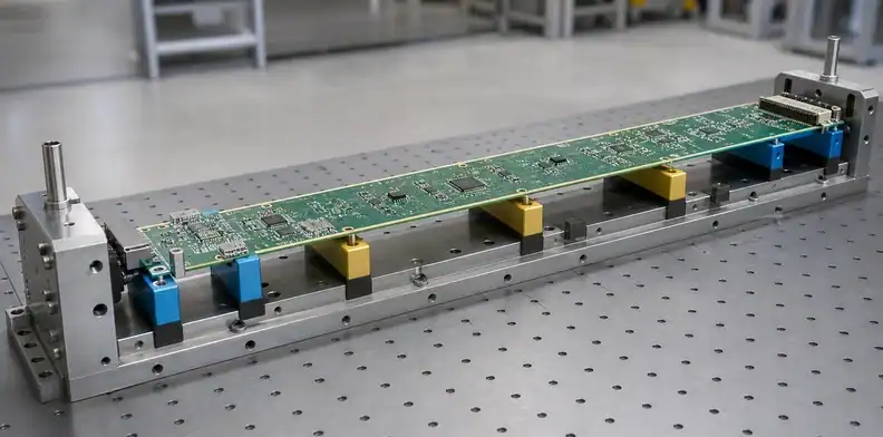
Quick Answer: Large PCB design should control four scale-dependent relationships before layout release: structural balance, functional datums, process support and long-distance electrical paths. Use a symmetric stack-up, review copper by region, dimension critical connectors from stable datums, reserve tooling/support edges and confirm the board’s layer-dependent process window. A layout that passes ordinary clearance rules can still fail because the large outline magnifies movement and tolerance accumulation.
Large PCB design rules are not ordinary layout rules enlarged to a wider canvas. The extra span changes how a small registration error appears at a connector, how an unbalanced copper region bends the board and how unsupported material moves through fabrication and assembly.
The most useful DFM review happens before routing is finished. It identifies the mechanical interfaces that control the product, the process features the supplier needs and the areas where electrical requirements limit copper balancing or datum changes. Those decisions give layout engineers boundaries they can actually use.
Table of Contents
- Set the process window before applying large PCB design rules
- Build a mechanically balanced stack-up
- Use functional datums for distant features
- Reserve edges for tooling and support
- Control copper and thermal distribution
- Route long signal and power paths deliberately
- Design for assembly, test and service
- Release the layout through a large-board DFM gate
Set the process window before applying large PCB design rules
Confirm the outline, layer count and required processes as one manufacturable combination before detailed layout. A maximum dimension published for a simple board does not automatically support the same length with a complex multilayer stack.
Prepare an early construction sheet with finished length and width, layer count, proposed material, finished thickness, copper weights, surface finish, impedance needs and special features. Mark items that are fixed by the product and items that may change after supplier review.
| Early input | Product-owned decision | Supplier return |
|---|---|---|
| Outline and datums | Functional envelope and mating interfaces | Usable process margin and tooling proposal |
| Stack and material | Electrical and regulatory boundary | Production stack and equivalency disposition |
| Copper and impedance | Current, loss and channel requirements | Compensation and test method |
| Assembly constraints | Component sides, mass and keep-outs | Carrier, travel and support route |
The process window should answer whether the board runs as a single unit or inside a temporary frame, which dimension controls equipment fit and where tooling or plating margin is needed. If a custom size is under review, keep an alternate partition or mechanical option available until the route is confirmed.
QueenEMS lists qualified large-board combinations on the large format PCB page. Use the companion maximum-size and layer-count decision to record the limiting process rather than treating raw sheet size as approval.
Layout should not consume every millimeter of the nominal field before the fabricator confirms edge needs. Keep critical copper, connectors and controlled features away from provisional process margins until CAM ownership is defined.
Build a mechanically balanced stack-up
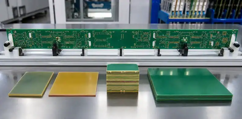
Balance material, dielectric spacing and copper weight around the centerline while preserving the electrical stack-up. An even layer count alone does not prevent a large board from bending.
Pair layers mechanically as well as electrically. Compare copper thickness, core and prepreg arrangement, resin demand and material family above and below the centerline. Avoid placing all heavy copper or broad planes in one half of the construction without an engineering reason.
Impedance requirements may constrain dielectric thickness and reference planes. Do not “fix” balance by moving a plane or changing prepreg without recalculating the channels. The goal is a stack that satisfies both structural and electrical requirements, with deviations documented and supported by the fabricator.
The PCB stack-up design guide provides the general construction logic. Large boards add greater sensitivity to panel movement, residual stress and free span. Ask the supplier to return the proposed production stack with actual material designations and finished copper assumptions.
Define substitution authority before the quote becomes an order. An equivalent material may be acceptable only if it preserves electrical properties, thermal behavior, flammability requirement, thickness and dimensional stability. A different prepreg that meets thickness but changes resin flow is not automatically equivalent.
Construction rule: Freeze the balanced stack-up and equivalency boundary before layout dimensions are treated as releasable.
Use functional datums for distant features
Dimension widely separated connectors, mounting holes and routed features from datums that represent the assembled product. Long chains of dimensions can accumulate error across the board even when every local feature meets its own tolerance.
Choose primary, secondary and tertiary references with the mechanical engineer. The primary datum may be a board surface or mounting plane. Secondary and tertiary datums can be tooling holes, locating slots or defined edges that constrain rotation and translation. The scheme should match how the board is located during inspection and final assembly.
Avoid using a routed corner as a precision origin without considering outline tolerance and burr condition. If connectors at opposite ends mate to a chassis, dimension them from a shared functional datum rather than from intermediate cutouts. Use slots or compliant hardware where the mechanical design needs controlled float.
Registration is a chain that includes inner-layer imaging, lamination movement, drilling, outer-layer imaging and routing. State which relationship is critical: hole to copper, connector hole to routed edge, gold finger to datum or pattern to enclosure. The PCB hole-position datum article helps convert a general tolerance into an inspectable requirement.
Request actual measurement evidence for production-critical relationships. A simple overall dimension report may not prove that the two connector fields are correctly located relative to the assembly datums.
Reserve edges for tooling and support
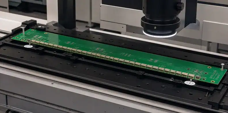
Large boards need a planned way to be gripped, registered, carried and tested without loading functional copper or components. Tooling edges are part of the manufacturing design, not leftover space.
Discuss whether the board needs removable rails, breakaway tabs, dedicated tooling holes, global fiducials or a carrier. Keep component bodies, exposed pads and critical traces clear of clamp and support zones. If the finished outline must contain components close to the edge, the assembly supplier may need a custom carrier.
Support requirements change by operation. Fabrication panels need registration and plating access. Solder paste printing needs underside contact. Reflow may need center support. Electrical test may apply probe load. One rail design may not solve every stage, so the process route should state when material is removed.
Tooling holes should not be confused with product mounting holes. Their size, tolerance and removal status need separate notes. The PCB tooling-hole requirements provide a baseline for supplier communication.
For extra-long boards, identify the preferred travel direction and lifting method. A board that fits the machine can still be damaged if operators lift it by one end. Reserve enough nonfunctional area for safe handling or specify a tray from first article onward.
Support call: Keep the required carrier, tooling edges and lifting zones free of functional features through the released revision.
Control copper and thermal distribution
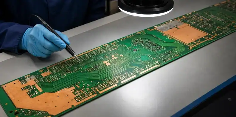
Review copper density globally, by mirrored layer pair and by local region. Large open areas beside dense power zones create different etching, stiffness and thermal behavior.
Generate copper-density views early enough to change placement or routing. Compare outer faces, mirrored internal layers and long transitions across the board. Look for one-sided planes, high-current bars, large keepout regions and isolated dense islands.
Functional copper controls the design. Ground and power planes may need to remain solid for return paths, shielding or current. Do not apply mesh solely because a forum says it reduces warp. Instead, coordinate plane distribution, connected fill and supplier-added thieving. Protect antennas, high-voltage clearances and impedance regions from automatic CAM fill.
The PCB copper-balance approval process defines who may add or change copper. Use the copper-thieving requirement article when nonfunctional process copper is permitted.
Component placement affects thermal distribution during assembly. Grouping shields, connectors and power devices in one area can slow heating through the oven and concentrate mechanical load in service. Electrical needs may prevent redistribution, but the assembly drawing should identify the risk for profiling and support.
Route long signal and power paths deliberately
Long physical routes require explicit delay, loss, return-path and voltage-drop decisions. Board size itself does not create poor performance; uncontrolled path length and reference changes do.
For high-speed interfaces, set maximum route lengths and skew based on the channel budget. Maintain continuous return paths and review every via, plane transition and connector. Longer routes may require a lower-loss laminate or different topology, but the material must remain available in the qualified large sheet and stack.
Use the controlled-impedance PCB specification to define target impedance, tolerance, stack-up ownership and test evidence. Place coupons where the production panel can support them; do not assume a standard coupon fits after the outline consumes most of the field.
For power distribution, calculate voltage drop and temperature rise along the actual path. Wider copper or heavier copper can help, but it changes etching and balance. Remote loads may benefit from local conversion or sensing rather than simply increasing copper everywhere.
Clock and synchronization paths across a long board need a deliberate topology. Connector fields and test access can introduce stubs. Review placement at system level before routing forces critical devices to opposite ends without a channel plan.
Electrical check: Accept the long layout only after delay, loss, return path and voltage drop are evaluated across the real distance.
Design for assembly, test and service
The board should be locatable, supportable, inspectable and repairable at its real size. A dense layout that fabricates successfully can still create an impractical assembly or service route.
Provide global and local fiducials appropriate to the assembly method. Keep conveyor or carrier edges usable. Identify bottom-side components that interfere with support. Place heavy parts near mechanical support where electrical and thermal design allow, and avoid making solder joints carry structural loads from connectors or heatsinks.
Test points need access and support underneath the board. A large fixture can apply enough force to flex an unsupported panel, causing false contacts or strain. Coordinate test-point fields with mounting and stiffener locations. The PCB design-for-test process helps decide which nets need fixture access and which can use functional or boundary-scan methods.
Serviceability may favor replaceable modules or wear interfaces. If the large continuous board remains necessary, protect high-cycle connectors and place diagnostic points where technicians can reach them without removing the full assembly.
Package and transport should be considered before the outline is frozen. Very long thin projections, unprotected corners and heavy edge hardware increase damage risk. A small outline change or removable shipment support can reduce that exposure.
Release the layout through a large-board DFM gate
Do not release material until mechanical, fabrication and assembly assumptions agree in one controlled package. Large-board DFM should close the issues that become expensive only after the panel is made.
Run a review using the final Gerber/ODB++, drill files, stack-up, fabrication drawing, assembly drawing and 3D/mechanical references. Include copper-density plots, impedance table, critical datums, tooling plan, flatness requirement, component-height map and test strategy.
Classify every supplier question:
- Release blocker: size/process incompatibility, missing outline, unapproved stack or critical datum conflict.
- Engineering approval: material substitution, copper modification, pad/clearance change or revised tooling edge.
- Supplier process decision: routine compensation or panel features within approved authority.
- Record only: clarification that does not change design intent or quotation.
The PCB DFM review before PO gives the commercial hold/release framework. For this large board, the output should also name the controlling process window and the evidence required at first article.
A contextual QueenEMS review can begin with the outline, stack-up, copper maps, datums and assembly constraints. The returned comments should identify manufacturability gaps and approval owners before tooling or laminate is committed.
For quotation, send the released manufacturing package, quantity breaks, inspection requirements and delivery destination. The quoted result should preserve the approved stack, tooling assumptions and critical mechanical relationships.
Use a release matrix to show which party controls each scale-sensitive feature. The PCB designer owns functional geometry, keep-outs and electrical intent. Mechanical engineering owns enclosure datums, mounting strategy and board support. The fabricator proposes production compensation and panel tooling within approved boundaries. The assembler owns fiducial use, carrier design, support pins and thermal profiling. Procurement should not approve a technical deviation merely because it changes price or lead time.
| Scale-sensitive feature | Primary owner | Evidence before release |
|---|---|---|
| Functional geometry and keep-outs | PCB design | Released manufacturing data |
| Enclosure datums and support | Mechanical engineering | Datum drawing and support model |
| Compensation and panel tooling | Fabricator | Approved CAM proposal |
| Carrier, fiducials and thermal route | Assembler | First-article process plan |
| Commercial deviation control | Procurement with engineering | Quote and signed disposition |
The final review should challenge four common failure patterns. First, a long connector row is dimensioned from a board edge even though the enclosure locates from mounting holes. Second, copper is locally dense near one end while the opposite side contains a large cutout. Third, support-pin access is blocked by bottom-side parts exactly where the board spans the conveyor. Fourth, a remote high-current load is routed through a narrow neck that meets ordinary design rules but creates unacceptable voltage drop and heat over distance.
Record how each large-board constraint will be checked. A carrier keep-out can be represented as a controlled region and checked against bottom-side component placement. The agreement between distant connector datums and the enclosure needs a mechanical comparison. Reflow movement needs a defined process check. Keep these results alongside the ordinary clearance and drill reports. A clean DRC result confirms the rules that were configured; it does not prove that an omitted support region or an unmodeled thermal condition is acceptable. Altium’s rule-system explanation describes how scope and configured constraints determine the checks performed.
Record the accepted solution beside the released revision. If copper balancing was authorized, preserve protected regions and the approved data source. If a carrier or stiffener is required, identify its interface and owner. If registration depends on a local datum or fiducial set, show it on the drawing used by inspection and assembly. These records prevent a repeat order from being rebuilt from informal CAM messages.
Treat any change to outline, layer count, laminate family, finished thickness, copper weight, large cutout, connector datum or assembly side as a trigger for review. A change that appears local can alter lamination behavior, panel utilization, support or line travel. The trigger list belongs in the engineering change process so the large-board controls survive after the first successful build.
For a design-rule review, send QueenEMS the final outline, stack-up and datum drawing together with copper maps, assembly constraints and quantity breaks. The response can separate release blockers, engineering approvals and supplier-controlled compensation before laminate or tooling is committed.
Release point: Manufacturing may start only when scale-sensitive datums, copper authority, support and evidence ownership are closed.

FAQ
Should every large PCB use a thicker laminate?
No. Thickness improves stiffness but can conflict with connectors, via geometry, impedance, weight and assembly. Select it from the complete mechanical and electrical system.
Are two global fiducials enough for a long PCB?
Not always. The assembly supplier may require a different global/local fiducial strategy when the board indexes or contains fine-pitch regions far apart.
Can the fabricator add copper for balance?
Yes, only within documented authority and protected-area rules. Functional planes, antennas, isolation and controlled-impedance regions may restrict additions.
Where should critical dimensions originate?
Use functional datums that represent how the board mates with the enclosure, connectors or fixture. Avoid long chains through unrelated features.
When should the supplier review the design?
Review the outline, stack-up and mechanical interfaces before detailed layout, then run final DFM on the released manufacturing package before the PO.
Sources
Written by the QueenEMS Engineering Team
Upload your files today · Free DFM check before production · Ship worldwide
Get your PCB prototypes in as fast as 24 hours. We handle FR4, Rogers, and hybrid boards up to 40 layers in volume production, with advanced builds subject to engineering review — free prototypes for 2–4 layer FR-4 boards, no minimum order.
Just upload your Gerber + BOM — we source every part, assemble, and inspect (AOI + X‑Ray) so you don't have to chase suppliers. Boards ship in as fast as 24 hours.