
Quick Answer: How to Choose Your HDI Type IPC-2226 classifies HDI boards into types based on microvia structures and sequential lamination cycles. Type I uses a 1+N+1 stackup starting around a 1.8x to 2.5x cost multiplier, Type II adds buried vias for 6-8 layers at a 3.0x multiplier, and Type III utilizes multiple microvia layers for 10+ layers, scaling up to 5.0x the standard cost.
Key Takeaways:
- Type I works best for >0.8mm BGA pitches with simple single-layer fanouts.
- Type II is mandatory when routing 0.5mm BGAs across 6-8 layers with buried vias.
- Type III handles dense <0.35mm pitch components but adds significant fabrication time.
- Always specify your required lamination cycle count explicitly in your factory RFQ.
Table of Contents
- #1 What Is IPC-2226 and Why Does HDI Type Matter?
- #2 What Is HDI Type I and When Should You Use It?
- #3 What Is HDI Type II and What Designs Actually Need It?
- #4 What Is HDI Type III and Is the Cost Premium Worth It?
- #5 How Do the IPC-2226 HDI Types Differ in Lamination Cycles?
- #6 What Are the Via Structure Rules for Each HDI Type?
- #7 How Does Your HDI Type Choice Affect Cost and Lead Time?
- #8 Which HDI Type Fits Your BGA Pitch and Layer Count?
- #9 How Do You Specify IPC-2226 HDI Type in Your Fabrication RFQ?
- #10 How Should You Future-Proof Your IPC-2226 HDI Type Selection?
Choosing the correct routing classification dictates the line between a profitable production run and a budget-destroying fabrication nightmare. Engineering teams often hit a wall where standard multilayer layouts fail under a tight BGA, forcing a transition into microvias and complex sequential lamination. You need to map component pitch and layer count directly to the correct factory stackup class. By matching your layout specifically to an IPC-2226 HDI type, you secure manufacturing yields and avoid overpaying for unnecessary laser drilling cycles.
#1 What Is IPC-2226 and Why Does HDI Type Matter?
IPC-2226 is the formal design standard classifying High Density Interconnect printed boards into types based on via structures and microvia layers. Selecting the correct type establishes your baseline manufacturing cost, which scales from 1.8x to over 5x standard board pricing because each type requires different factory processes.
Defining the Global Standard
IPC-2226A “Sectional Design Standard for High Density Interconnect (HDI) Printed Boards” operates as the official framework defining HDI classification across the electronics industry. It categorizes boards into distinct classes, dictating exactly how factories must structure blind, buried, and microvias. This standardization prevents miscommunication between designers and fabrication floors.
Consider this basic classification:
- Type 0 represents standard multilayer boards without microvias.
- Type I incorporates a single layer of microvias on the outer surfaces.
- Type II adds buried vias spanning the core layers.
- Type III introduces multiple microvia layers that can be stacked.
The Hidden Baseline Category
Many engineering texts ignore the Type 0 designation, leading to confusion when evaluating base costs. Type 0 is standard multilayer fabrication, relying entirely on mechanically drilled through-holes. Recognizing this baseline helps you validate whether your design actually requires microvias before committing to sequential lamination.
Key Takeaway: Recognizing the official classification system allows you to communicate exact stackup expectations with your fabrication partner. Bottom line: Always evaluate your routing against Type 0 limits before upgrading your layout to higher density classes.
| Feature | Type 0 (Standard) | Type I (1+N+1) | Type II (2+N+2 style) | Type III |
|---|---|---|---|---|
| Microvia Layers | 0 | 1 | 1 (per side) | 2 or more |
| Buried Vias | No | No | Yes | Yes |
| Lamination Cycles | 1 | 2 | 3 | 4+ |
| Cost Multiplier | 1.0x | 1.8x – 2.5x | 2.5x – 3.5x | 3.5x – 5.0x |
| Target BGA Pitch | >0.8mm | 0.5mm – 0.8mm | 0.4mm – 0.5mm | <0.35mm |
Analyzing this table reveals how each step up the classification ladder directly inflates both cycle times and unit costs.
#2 What Is HDI Type I and When Should You Use It?
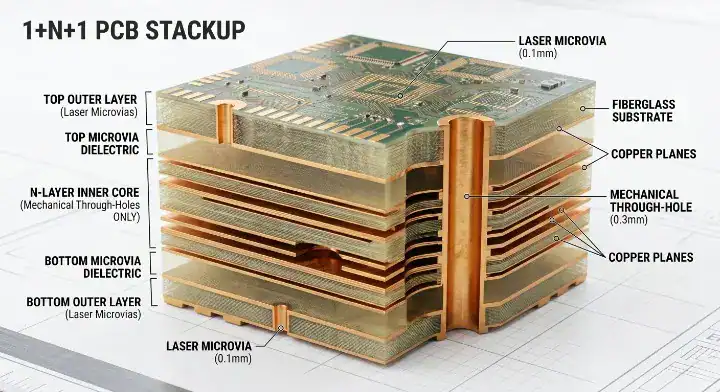
HDI Type I features a single microvia layer built on top of a standard multilayer core, establishing a basic 1+N+1 stackup configuration. It costs roughly 1.8-2.5x more than a standard multilayer board and supports BGA pitches down to 0.5mm.
Structuring the 1+N+1 Layout
Type I is the entry-level high-density configuration. It utilizes laser-drilled microvias connecting layer 1 to layer 2, and layer N to layer N-1, without any buried vias in the core. The entire inner core is pressed together in one cycle, followed by the outer microvia layers in a second cycle.
Here is what defines this structure:
- Only one laser-drilled microvia layer exists per side.
- Through-holes span the entire board thickness.
- The factory performs exactly two lamination cycles.
Identifying Best Fit Applications
You should target this classification when routing moderate-density components that exceed standard mechanical drilling limits. Devices utilizing single-chip microcontrollers or basic memory modules fit perfectly into this category. Specifying the correct via fill copper or resin choice keeps the outer layers flat for reliable component soldering.
Key Takeaway: The 1+N+1 structure offers the most affordable entry point into high-density routing by limiting the press cycles. Bottom line: Use Type I to escape standard mechanical drill limits without paying for internal buried via processing.
#3 What Is HDI Type II and What Designs Actually Need It?
HDI Type II utilizes one microvia layer combined with buried vias that span multiple core layers, fitting 6-8 layer designs perfectly. It costs 2.5-3.5x a standard board because it requires three lamination cycles, which means fabrication complexity increases significantly.
Differences Between Type II and Type III
Many designers ask what specifically separates these two middle classifications. Type II has exactly one microvia layer on the outer surfaces, and these microvias do not span multiple layers vertically. Type III possesses two or more microvia layers, allowing vias to stack or stagger across multiple sequential levels. This boundary determines how aggressive your fanout strategy can be.
Let’s break that down:
- Type II easily handles 6-8 layer boards needing buried via channels.
- Type III becomes necessary for 10+ layers and fine-pitch BGAs.
- Upgrading from Type II to Type III increases costs by 30-40%.
- Pitches below 0.5mm frequently force a transition into Type III.
Recognizing the Routing Demands
You should deploy Type II when internal signal congestion blocks standard through-hole routing. The addition of buried vias allows inner traces to cross without piercing the outer layers, freeing up premium surface area. Reviewing the 7 signals you need HDI design clarifies when standard multilayers fail and buried vias become mandatory.
Key Takeaway: Adding buried vias creates massive internal routing channels but forces an additional core pressing cycle. Bottom line: Specify Type II for dense 6-8 layer layouts where internal signal routing requires dedicated buried via paths.
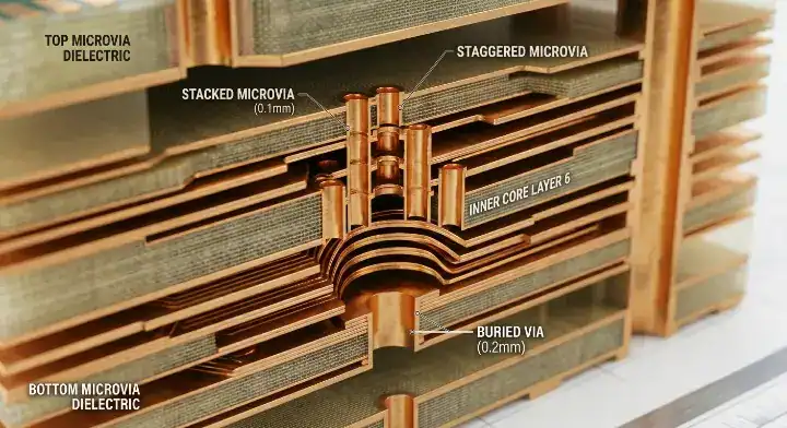
#4 What Is HDI Type III and Is the Cost Premium Worth It?
HDI Type III features two or more microvia layers with stacked or staggered structures, costing 3.5-5x a standard printed board. It supports ultra-dense 10+ layer designs and <0.35mm pitch packages because it allows intricate vertical fanouts, resulting in maximum space utilization.
Is ELIC the Same as Type III?
Buyers frequently experience confusion when vendors swap terms interchangeably during quoting. ELIC (Every-Layer Interconnect) is an extreme subset of Type III, not a direct synonym for the entire category. Standard Type III uses 2-3 microvia layers alongside buried vias, while ELIC features microvias connecting every single adjacent layer pair.
Watch out for these cost dynamics:
- Standard Type III runs approximately 3.5x the baseline cost.
- Type III with stacked microvias pushes the premium to 4-5x.
- True ELIC manufacturing commands a massive 5-7x cost multiplier.
- Vendors often mix these labels, requiring strict RFQ documentation.
Real Production Capabilities
On our floor, we run Standard Type III and Type III with 2-level stacked microvias as core production capability. Full ELIC is a different conversation—it requires 7-9 lamination cycles, every-layer microvia interconnection, and process tolerance discipline that takes years to build. Across the global HDI industry, we estimate fewer than 30 facilities can stably produce ELIC at production volume. We see customers come to us after a cheaper vendor accepted their ELIC order but failed the first production lot at 23% yield.
Key Takeaway: The structural differences inside the Type III category dictate extreme variations in factory pricing and yield risk. Bottom line: Budget for a 5-7x cost multiplier if your smartphone or GPU layout genuinely needs ELIC, and strictly verify your vendor’s track record.
| Classification | Microvia Configuration | Lamination Cycles | Cost Premium | Target Application |
|---|---|---|---|---|
| Standard Type III | 2-3 microvia layers, staggered | 4-5 cycles | 3.5x – 4.0x | Server boards, 5G base stations |
| Type III Stacked | 3-level stacked microvias | 5-6 cycles | 4.0x – 5.0x | Complex EV BMS, high-end IoT |
| Full ELIC | Microvias on every layer | 7-9 cycles | 5.0x – 7.0x | Smartphone mainboards, AI substrates |
This cost breakdown proves why matching your exact density requirements to the correct Type III subclass is mandatory for budget control.
#5 How Do the IPC-2226 HDI Types Differ in Lamination Cycles?
The IPC-2226 HDI types require varying sequential lamination cycles, starting at two cycles for Type I and scaling up to seven or more for ELIC. Each additional press cycle adds 15-20% to your fabrication invoice because it forces the factory to repeat pressing, drilling, and plating processes.
Counting the Press Steps
Every time a factory adds a new layer of microvias or buried vias, the core must go back into the lamination press. Type I requires pressing the core, then pressing the outer prepreg layers, totaling two cycles. Type II demands pressing the inner core, drilling the buried vias, pressing the next layers, and then laser drilling the microvias.
Here is how the cycles accumulate:
- Standard Type 0 requires 1 press cycle.
- Type I configurations demand 2 cycles.
- Type II setups require exactly 3 cycles.
- Type III designs start at 4 cycles and scale rapidly.
Minimizing Sequential Operations
You can control your budget by intentionally restricting the number of times your board enters the lamination press. Engineers often over-specify stackups, adding cycles that their routing density does not actually demand. Implementing strategies to reduce HDI sequential lamination cost helps keep the project within viable commercial boundaries.
Key Takeaway: Sequential lamination is the primary driver of high-density manufacturing expenses and extended factory lead times. Bottom line: Keep your lamination cycles to a maximum of three unless your BGA pitch explicitly demands more complex stacking.
#6 What Are the Via Structure Rules for Each HDI Type?
Each IPC-2226 HDI type dictates strict via combinations, such as Type I relying exclusively on blind and through-hole vias, while Type II introduces buried structures. Following these designated geometric rules validates your board against IPC-6012E Class 3 reliability standards.
Validating Aspect Ratios
IPC-6012E Rigid PCB Performance Specification requires high-density products to pass strict thermal simulation tests to verify via integrity. To meet these demands, factories limit the depth of laser-drilled holes relative to their diameter. An aspect ratio of ≤1:1 is standard across all classes, meaning a 0.1mm microvia cannot penetrate deeper than 0.1mm into the dielectric.
Consider these structural constraints:
- Microvia aspect ratios must never exceed 1:1.
- Staggered microvias require precise lateral offset distances.
- Stacked vias demand perfectly flat copper plating on the target pad.
- Buried vias must utilize reliable resin filling processes.
Choosing Between Stacked and Staggered
The internal arrangement of multiple microvia layers severely impacts long-term thermal reliability. Staggering vias across different locations on adjacent layers disperses mechanical stress, while stacking them directly on top of each other concentrates thermal expansion forces. Analyzing stacked vs staggered microvia for BGA reliability reveals why factories prefer staggering whenever routing space permits.
Key Takeaway: Maintaining strict aspect ratios prevents plating failures deep inside the laser-drilled holes. Bottom line: Calculate your dielectric thickness carefully to guarantee your microvias stay within the ≤1:1 aspect ratio limit.
#7 How Does Your HDI Type Choice Affect Cost and Lead Time?
Choosing your IPC-2226 HDI type directly dictates your budget and factory schedule, scaling from a 2.1x cost and 14 days for Type I up to a 5.8x cost and 35 days for full ELIC. Specifying a higher classification than your routing actually requires immediately inflates unit pricing and delays market entry.
Analyzing Quoting Data
We tracked quoting multipliers across our 2024-2025 production data to give engineering teams accurate baselines. Compared to a standard 6-layer FR-4 board at a $1.00 normalized base, Type I averages 2.1x, and Type II lands at 3.0x. Pushing into Standard Type III runs 3.8x, Type III with 2-level stacked microvia hits 4.4x, and full ELIC reaches 5.8x.
What does this mean for your schedule?
- Standard boards ship in 7-10 days.
- Type I extends delivery to 10-14 days.
- Type II schedules require 14-18 days.
- Type III designs need 18-25 days.
- ELIC pushes lead times to 25-35 days.
Factory Realities on Over-Specification
Customers who push too aggressively toward higher categories often realize six months into production that they overpaid. They could have hit their exact density targets with Type II simply by accepting a slightly larger board outline. Evaluating the microvia aspect ratio sweet spot allows designers to maximize lower-tier structures before jumping to the next cost bracket.
Key Takeaway: Every step up the standard classification ladder adds roughly five days to your fabrication lead time. Bottom line: Run the cost trade-off between increasing your board outline size versus paying for a higher HDI classification.
#8 Which HDI Type Fits Your BGA Pitch and Layer Count?
A 0.4mm pitch BGA typically dictates Type II or Type III depending on your fanout density, while >0.8mm components safely operate in Type 0 or Type I territory. Aligning your selected class directly with your physical layer count prevents over-engineering and keeps fabrication highly efficient.
Can You Downgrade From Type II to Type I?
Many layout engineers want to downgrade their stackup to save money after receiving high factory quotes. You can successfully drop from Type II to Type I, saving 25-30% on fabrication, but only under strict physical conditions. Your layer count must remain at six or fewer, you cannot use buried vias, and your tightest BGA pitch must be ≥0.65mm.
Here are the downgrade risks:
- Redesigning without buried vias increases board area by 8-15%.
- Routing complexity rises sharply on the outer layers.
- You must verify if the area increase offsets the fabrication savings.
Case Study: Optimizing High-Density Layouts
An IoT startup in Seattle sent us a 10-layer wearable health tracker featuring a 0.4mm pitch SiP module. Their layout team specified Type III with 3-level stacked microvias, assuming finest pitch needed the finest HDI tier. We reviewed the files and proposed Type II with 2-level stacked microvias only in the SiP fanout region, transitioning to staggered vias elsewhere. Total lamination cycles dropped from five to three, dropping unit cost from $11.40 to $7.20 while improving D-coupon reliability yields.
Key Takeaway: Higher density classifications are not inherently better; they are simply tools to solve specific component geometry problems. Bottom line: Map your tightest BGA pitch directly to the required HDI class before setting up your CAD design rules.
| Application Domain | Typical BGA Pitch | Recommended HDI Classification | Expected Layer Count |
|---|---|---|---|
| Industrial Controllers | 0.8mm – 1.0mm | Type 0 or Type I | 4 – 6 Layers |
| Medical Wearables | 0.4mm – 0.5mm | Type II | 6 – 8 Layers |
| Automotive EV BMS | 0.4mm – 0.65mm | Type II or Standard Type III | 8 – 12 Layers |
| High-Speed Servers | 0.35mm – 0.5mm | Standard Type III | 12 – 18 Layers |
| 5G Smartphones | <0.35mm | Full ELIC | 10 – 14 Layers |
This matrix proves that application demands, not arbitrary design choices, should dictate your final stackup configuration.

#9 How Do You Specify IPC-2226 HDI Type in Your Fabrication RFQ?
Specifying the IPC-2226 HDI type in your factory RFQ requires explicitly stating the lamination cycle count, the microvia aspect ratio limits, and your testing requirements. Providing exact documentation prevents vendors from misinterpreting your intended stackup and quoting an under-qualified, failure-prone manufacturing process.
Drafting Clear Fabrication Notes
IPC-2221B Generic Standard on Printed Board Design defines the universal layout rules that apply to all circuit board designs. You must build upon these basics by clearly defining your high-density requirements in your fabrication drawings. Never assume a factory will infer your required class just by looking at the drill files.
Follow these exact RFQ steps:
- Write “IPC-2226 Type II” (or your specific class) directly in the fab notes.
- Request a breakdown of the exact lamination cycle count.
- Detail the acceptable aspect ratio for all microvias.
- Ask for recent case studies and IPC TM-650 test reports.
- Order a 10-25 piece qualification lot with first article inspection.
Recognizing Vendor Red Flags
You must aggressively vet factories claiming they can handle advanced stackups at massive discounts. If a fabrication quote comes back 30% lower than the industry average, the vendor is likely quoting a Type II process while calling it Type III. Require physical evidence, such as microvia cross-section photos from past projects, to validate their production claims.
Key Takeaway: Ambiguous fabrication notes allow unqualified vendors to accept orders they cannot reliably manufacture. Bottom line: Demand documented D-coupon testing capabilities and first article inspection reports before placing high-density volume orders.
#10 How Should You Future-Proof Your IPC-2226 HDI Type Selection?
Future-proofing your IPC-2226 HDI type selection means validating the minimum viable stackup now while leaving layout space for subsequent component density upgrades. This engineering approach prevents total board redesigns and stabilizes your per-unit manufacturing cost across multiple product generations.
Planning for the Next Generation
Designing a product platform requires anticipating the dimensions of next year’s silicon packages. If you currently rely on a HDI stackup choices 1+N+1 vs 2+N+2 vs ELIC decision, you need to know how scaling down to a 0.35mm pitch will affect the existing layout. Leaving slightly larger BGA fanout zones today allows you to drop in smaller chips later without bumping the entire board up to Type III.
Consider this scaling strategy:
- Start with Type I if your initial chips allow it.
- Route critical signals to avoid creating artificial chokepoints.
- Maintain clear channels to allow buried vias if an upgrade to Type II becomes necessary.
- Avoid stacked vias entirely until layer counts force their use.
Partnering for Long-Term Success
Early engineering collaboration with your fabrication facility prevents severe scaling issues. When designers share their product roadmaps with our engineering team, we structure the initial Type II board so it can easily transition into a standard Type III layout for the next hardware revision. This foresight saves months of layout time when marketing demands a smaller enclosure.
Key Takeaway: Strategic stackup planning allows your circuit boards to accommodate tighter component pitches without exploding the fabrication budget. Bottom line: Lock in your stackup classification based on current component data, but map out the exact cost impact of jumping to the next tier.
Conclusion
At QueenEMS, we believe that choosing the right microvia classification should be driven by precise engineering data, not vendor marketing terms. We offer free DFM/DFA engineering reviews and provide full 3D AOI and X-Ray inspection on every high-density BGA joint to validate your stackup design. Whether you are scaling up a Type II medical wearable or validating a complex ELIC smartphone board, contact us today to stabilize your production yields.
FAQ
What is the difference between HDI Type II and Type III?
Type II has exactly one microvia layer combined with buried vias that span multiple layers. Type III features two or more microvia layers with stacked or staggered structures, allowing for much denser routing. Use Type II for 6-8 layer boards with BGA pitches >0.5mm, and transition to Type III for 10+ layers with tighter pitches, keeping in mind the 30-40% cost increase. Send your files for a stackup review to lock in the right class.
Is ELIC the same as IPC-2226 Type III HDI?
No, ELIC is not a direct synonym. ELIC (every-layer interconnect) is an extreme subset of Type III where every adjacent layer pair features microvia connections, while standard Type III only uses 2-3 microvia layers. ELIC demands a massive 5-7x cost premium compared to standard boards, and very few global facilities can manufacture it reliably. Always specify your exact layer-to-layer connections in your RFQ.
Can I downgrade from HDI Type II to Type I to save money?
Yes, downgrading is possible if your layer count remains ≤6 and you can replace all buried vias with standard through-holes. Making this change saves roughly 25-30% on fabrication costs, but it frequently increases the physical board area by 8-15% due to restricted routing channels. Calculate whether the cost savings outweigh the area penalty before rewriting your design rules.
How do I verify my fab can actually produce Type III HDI?
Request specific documentation including recent Type III case studies with cross-section photos, IPC TM-650 2.6.27A test reports, and their D-coupon testing capability statement. If a vendor quotes prices 30% below the industry average, they might be attempting to pass off a Type II process as Type III. Run a small qualification lot with a first article inspection before committing to volume production.
What HDI Type does a 0.4mm pitch BGA require?
A 0.4mm pitch BGA typically requires a Type II or Type III classification depending heavily on your total signal density and layer count. For simple fanouts on boards with ≤8 layers, Type II often provides enough routing flexibility. For complex 10+ layer boards with tight component grouping, you will likely need Type III featuring 2-level stacked microvias. Let our engineering team verify your layout limits today.
Upload your files today · Free DFM check before production · Ship worldwide
Get your PCB prototypes in as fast as 24 hours. We handle FR4, Rogers, and Flex up to 60 layers — free prototypes for 2–4 layer boards, no minimum order.
Just upload your Gerber + BOM — we source every part, assemble, and inspect (AOI + X‑Ray) so you don't have to chase suppliers. Boards ship in as fast as 24 hours.