
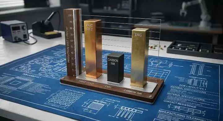
Quick Answer: Carbon ink is a cost-effective conductive coating applied to PCB contact pads and traces, reducing surface finish expenses by 60–80% compared to electrolytic hard gold. It handles over 1,000,000 mechanical actuation cycles and provides sheet resistances ranging from 5 Ω/sq to 1 MΩ/sq, making it highly effective for membrane switches, remote controls, and industrial keypads. Key takeaways:
- Cuts keypad surface finish costs up to 73% per board.
- Achieves ±8% resistance tolerance using strict viscosity control.
- Cannot be soldered; strictly for mechanical contact interfaces.
- Ideal for flexible polyimide substrates due to high elasticity.
Table of Contents
- What Is Carbon Ink and Why Does It Matter for PCB Cost?
- How Is This Conductive Paste Applied to a Board Surface?
- What Controls Carbon Ink Resistance on Your PCB?
- How Does Printed Carbon Compare to Hard Gold and ENIG?
- Can You Solder Components on Carbon Ink Pads?
- Where Do Engineers Apply Conductive Carbon in Real Products?
- What Are the Real Tolerance Limits of Printed Resistors?
- How Do You Design PCB Pads for Carbon Oil Printing?
- What Makes Carbon Paste Ideal for Flexible and Wearable Boards?
- When Should You Avoid Carbon Ink on Your Board?
Many hardware teams face severe budget overruns when specifying hard gold for large membrane switch panels or multi-button controllers. Specifying expensive electrolytic gold for simple keypad contacts drains project budgets unnecessarily, especially in high-volume production. Carbon ink is a screen-printed conductive layer that replaces gold on contact pads, dropping surface finish costs by up to 80% while passing strict durability tests. When you use our rapid PCB prototyping services, you can physically test these conductive carbon circuits in your custom product housing within just a few days.
What Is Carbon Ink and Why Does It Matter for PCB Cost?
Carbon ink provides a highly durable, 0.5-mil thick conductive protective layer for PCB contact points, costing only $0.05 to $0.15 per board depending on the printed area. Because gold prices continuously fluctuate, replacing hard gold contacts with printed carbon paste directly cuts your bill of materials (BOM), resulting in massive savings for consumer electronics. Conductive carbon ink is a polymer thick film composed of graphite particles suspended in an epoxy resin. It withstands 1,000,000 actuation cycles on standard membrane switches.
Primary Material Composition
The performance of the printed layer depends entirely on its chemical makeup. High-quality pastes mix fine carbon powder with specific resin binders and solvents.
- Carbon particles: Provide the conductive pathways.
- Resin binder: Creates adhesion to the FR4 or polyimide substrate.
- Solvents: Control viscosity during the printing stage.
Cost Reduction Mechanics
Here is the reality: electrolytic hard gold requires expensive chemical baths and electrical bus lines tied to every single pad. Printing a carbon-based paste removes the need for bus lines and uses a simple additive screen printing method.
Key Takeaway Bottom line: Switch to printed carbon for user interfaces and keypads to immediately reduce your board’s surface finish expenditures by at least 60%.
| Feature | Hard Gold | Printed Carbon Paste |
|---|---|---|
| Process Type | Electrolytic plating | Screen printing |
| Relative Cost | Very High | Low |
| Typical Use | High-wear edge connectors | Keypads, simple switches |
| Cost comparison indicates carbon paste offers significant financial advantages for non-critical contact points. |
How Is This Conductive Paste Applied to a Board Surface?
Engineers apply the conductive paste using a precision silkscreen process that deposits a 0.3 to 1.0-mil thick layer onto designated copper pads. This happens late in the manufacturing cycle, typically after the primary surface finish (like HASL or ENIG) is applied to the rest of the board. The paste goes through a thermal curing phase to solidify the resin and lock the conductive particles in place.
The Screen Printing Workflow
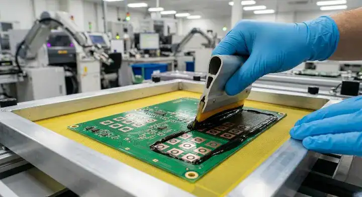
To achieve precise application, operators use a specialized mesh stencil. The stencil openings define exactly where the material will land on the printed circuit board.
- A squeegee forces the paste through the mesh onto the PCB.
- Boards enter a baking oven at 150-170°C.
- Curing lasts 30 to 60 minutes to evaporate solvents completely.
Quality Control and Curing
Consider this: incomplete curing leaves the paste soft, which means contact resistance will drift over time. Proper thermal profiling creates a hard, stable surface that resists friction from rubber keypads.
Key Takeaway Bottom line: Always specify a post-curing baking temperature of 150-170°C for at least 30 minutes to guarantee mechanical hardness and electrical stability.
| Process Step | Parameter | Expected Result |
|---|---|---|
| Printing | Mesh size 100-120T | Precise edge definition |
| Baking | 150-170°C | Solvent evaporation |
| Curing Time | 30-60 minutes | Maximum adhesion |
| Strict adherence to thermal parameters dictates the final mechanical strength of the printed layer. |
What Controls Carbon Ink Resistance on Your PCB?
The final resistance of carbon ink depends strictly on the paste formulation, the printed thickness (0.3-1.0 mil), and the physical dimensions of the printed area. Many engineers on the Electronics Stack Exchange and Patent CN104519671B discussion forums struggle with resistance deviations caused by uneven print thickness. You must calculate sheet resistance using the formula R = ρ × L / (B × H), where thickness (H) is the most critical variable to control during fabrication.
Addressing Resistance Drift
According to the MDPI Coatings Journal review of carbon-based conductive inks, sheet resistance ranges dynamically from 5 Ω/sq to 1 MΩ/sq. Controlling this range requires rigorous factory protocols.
At QueenEMS, we use four-probe testing equipment to measure sheet resistance on every printed panel before shipping. One recurring client problem was ink viscosity drift during long production runs—solvent evaporation gradually increased viscosity, resulting in thicker deposits and lower resistance. We instituted a mandatory viscosity check every 2 hours, maintaining the paste within ±5% of the target range. This protocol improved our batch-to-batch resistance consistency from ±18% down to ±8%, meaning clients receive boards matching their exact design specifications.
Key Takeaway Bottom line: You must partner with a manufacturer that utilizes continuous viscosity monitoring and four-probe testing to prevent mid-batch resistance variations.
| Variable | Influence on Resistance | Factory Tolerance |
|---|---|---|
| Paste Viscosity | High | ±5% control |
| Print Thickness | High | ±0.3 mil |
| Baking Temp | Medium | ±5°C |
| Variations in thickness directly alter the conductive cross-section, causing significant electrical drift. |
How Does Printed Carbon Compare to Hard Gold and ENIG?
Printed carbon provides superior cost efficiency for friction-based contacts, while hard gold delivers lower electrical resistance and ENIG provides the flattest solderable surface. Per the IPC-6012F standard, any surface finish must meet strict qualification metrics for its specific class. While you might read an ENIG surface finish guide for component placement, printed paste is strictly for mechanical interfaces.
Application Differences
Engineers often struggle to choose between finishes for complex user interfaces. Understanding the chemical and mechanical limits simplifies the decision.
- Hard gold withstands heavy edge-connector insertion friction.
- ENIG provides highly planar pads for fine-pitch BGAs.
- Carbon paste dominates rubber keypad interfaces.
Financial and Operational Trade-offs
Here is the reality: using gold for simple button contacts wastes money. When you review a HASL vs ENIG surface finish comparison, you see that neither handles millions of rubber button presses as cost-effectively as printed paste.
Key Takeaway Bottom line: Reserve hard gold strictly for edge connectors and use printed paste for all membrane or rubber keypad contacts to maximize budget efficiency.
| Finish Type | Best Application | Solderability |
|---|---|---|
| Hard Gold | Edge connectors | Poor |
| ENIG | Fine-pitch SMD | Excellent |
| Printed Paste | Keypad contacts | None |
| Selecting the correct finish requires balancing contact friction requirements against assembly demands. |
Can You Solder Components on Carbon Ink Pads?
No, you cannot solder components onto carbon ink pads because the polymer resin binder repels liquid solder and contains no metallic structure for an intermetallic bond to form. Users on the Music Electronics Forum and PCB International tech notes frequently ask why their solder joints fail on these black pads. The paste acts purely as a mechanical contact interface or printed resistor, resulting in complete solder rejection during wave or reflow processes.
Assembly Compatibility
Because the paste cannot be soldered, your assembly team must treat these boards carefully. The printed areas must be kept clean of flux residues.
- Flux cleaners can degrade the epoxy resin binder.
- High reflow temperatures can alter the cured resistance values.
- Masking might be required during aggressive wave soldering.
Avoiding Design Errors
Consider this: routing an SMD resistor footprint and specifying it for paste printing will ruin your assembly phase. You must separate your contact interfaces from your component mounting zones entirely.
Key Takeaway Bottom line: Never place SMD or through-hole component footprints on printed paste areas; use standard finishes like HASL or ENIG for all soldered connections.
| Assembly Process | Compatibility | Risk Level |
|---|---|---|
| Reflow Soldering | None | High (Resistance drift) |
| Wave Soldering | None | High (Thermal shock) |
| Flux Cleaning | Poor | Medium (Resin degradation) |
| Exposure to standard SMT thermal profiles can negatively shift the electrical properties of the cured paste. |
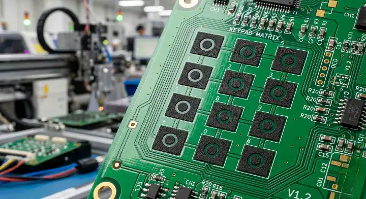
Where Do Engineers Apply Conductive Carbon in Real Products?
Engineers apply conductive carbon to television remote controls, industrial membrane keyboards, automotive steering wheel controls, and low-current jumper traces. It acts as a highly resilient contact surface that bridges the gap between copper traces and conductive rubber plungers. Because it naturally resists oxidation, it performs exceptionally well in humid environments where exposed copper would fail rapidly.
Real-World Cost Engineering
A consumer electronics client came to us with a TV remote design using ENIG on the keypad pads, bringing their BOM cost to $0.45 just for the finish. We proposed switching those 24 keypad pads to printed paste while keeping ENIG only on the 6 BGA pads. This hybrid approach reduced their finish cost to $0.12 per board—a 73% reduction. We delivered 50,000 units with zero field failures reported, validated through our 1-million-cycle push-button endurance test.
Industrial Applications
Beyond consumer remotes, industrial designers rely on this process for rugged interfaces. The thick film prevents mechanical wear from heavy-handed operators.
- HVAC control panel interfaces.
- Medical device membrane keypads.
- Security system access keypads.
Key Takeaway Bottom line: Specify hybrid surface finishes—paste for keypads and ENIG for BGAs—to optimize both interface durability and SMT assembly yields.
| Product Type | Primary Function | Actuation Cycles |
|---|---|---|
| TV Remote | Button contacts | > 1,000,000 |
| HVAC Panel | Membrane switch | > 500,000 |
| Automotive | Steering controls | > 2,000,000 |
| High-actuation devices benefit immediately from the superior mechanical wear resistance of polymer thick films. |
What Are the Real Tolerance Limits of Printed Resistors?
Carbon ink resistors achieve a standard tolerance of ±10% to ±30%, with a Temperature Coefficient of Resistance (TCR) hovering around ±200 ppm/°C. According to Auspi Enterprises technical analyses and various engineering forums, designers often mistakenly attempt to replace precision ceramic resistors with printed paste. While embedded resistor PCB technology offers advanced integration, standard printed paste resistors are restricted to simple current limiting or pull-up/pull-down functions.
Design Limitations
Because the tolerance is wide, you cannot use these resistors for timing circuits or voltage references. The printing squeegee pressure introduces minor thickness variations across the panel.
- Unsuitable for analog-to-digital converter (ADC) references.
- Unsuitable for high-frequency RF terminations.
- Acceptable for basic LED current limiting.
Environmental Drift
Here is the reality: humidity and extreme temperature cycling will shift the resistance value over time. The epoxy binder absorbs minute amounts of moisture, which slightly pushes the conductive particles apart.
Key Takeaway Bottom line: Only use printed resistors for non-critical logic pull-ups or LED limiters where a ±20% resistance shift will not affect circuit functionality.
| Specification | Typical Value | Limitation |
|---|---|---|
| Tolerance | ±10% to ±30% | Too wide for precision |
| TCR | ±200 ppm/°C | Drifts in extreme heat |
| Best Use Case | Pull-up networks | Non-critical timing |
| Standard silkscreen processes cannot match the ±1% precision offered by dedicated surface mount ceramic resistors. |
How Do You Design PCB Pads for Carbon Oil Printing?
Designing PCB pads for carbon oil requires making the paste area 6 to 8 mils larger than the underlying copper pad to prevent copper oxidation. The minimum printable line width for the paste is 100μm, and typical keypad contact diameters range from 2mm to 8mm. You must provide your manufacturer with a dedicated Gerber layer specifically outlining the paste shapes to guarantee precise stencil creation.
Overlap and Spacing Rules
Because the paste must completely seal the copper from the atmosphere, overlap is strictly required. Failing to overlap the copper will lead to edge corrosion.
- Extend paste 6-8 mils beyond copper edges.
- Maintain a minimum of 10 mils clearance between adjacent printed pads.
- Keep paste 10 mils away from standard solder mask openings.
Secondary Printing Requirements
Consider this: if your design requires crossing traces, you can use the paste as a low-cost jumper over a dielectric layer. If performing a second paste print, the secondary graphic must be 2-3 mils smaller than the first to accommodate alignment tolerances.
Key Takeaway Bottom line: Always design your paste CAD layer to be oversized by at least 6 mils compared to the copper pad to establish a perfect anti-oxidation seal.
| Design Parameter | Minimum Requirement | Purpose |
|---|---|---|
| Paste Overhang | 6-8 mils | Prevents edge oxidation |
| Trace Width | 100 μm | Manufacturability limit |
| Pad Clearance | 10 mils | Prevents short circuits |
| Strict adherence to overlap rules prevents environmental moisture from attacking the underlying copper structures. |
What Makes Carbon Paste Ideal for Flexible and Wearable Boards?
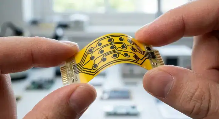
Carbon paste is highly elastic due to its epoxy resin binder, allowing it to bend repeatedly without cracking or losing electrical continuity on polyimide substrates. When you work with a flexible PCB manufacturer, they often recommend this paste for wearable devices because traditional metallic finishes like hard gold can fracture under tight bending radiuses. The printed paste flexes naturally with the substrate, resulting in highly reliable dynamic flex circuits.
Wearable Device Applications
Smart clothing and medical wearables require circuits that move with the human body. The paste handles physical deformation gracefully.
- Biometric sensor contact points on skin.
- Foldable electronic joints.
- Heater elements in smart jackets.
Dynamic Flex Durability
Here is the reality: rigid metallic plating flakes off polyimide when subjected to continuous dynamic folding. The polymer thick film stretches and compresses, maintaining a stable conductive matrix even at a 180-degree crease.
Key Takeaway Bottom line: Specify printed conductive paste for any flexible circuit contact points that will experience continuous bending or twisting in the final product.
| Substrate | Paste Adhesion | Bending Performance |
|---|---|---|
| FR4 (Rigid) | Excellent | N/A |
| Polyimide (Flex) | Excellent | High elasticity |
| PET (Flex) | Very Good | Good elasticity |
| The innate flexibility of the polymer binder makes it the superior choice for dynamic flex circuit applications. |
When Should You Avoid Carbon Ink on Your Board?
You must avoid carbon ink on any PCB areas requiring component soldering, precision analog voltage references, or high-frequency RF transmission. Because the sheet resistance is relatively high and variable, placing it in a high-speed digital signal path will cause severe impedance mismatches, which means signal reflections will corrupt your data. The paste is strictly designed for direct mechanical actuation and low-frequency electrical conduction.
High-Frequency Limitations
High-frequency signals require continuous, highly conductive copper planes and traces. The granular nature of graphite particles creates parasitic capacitance and resistance.
- Do not use on PCIe or HDMI data lines.
- Avoid placing near RF antenna feedlines.
- Never use as a primary power distribution trace.
Precision Analog Constraints
Consider this: analog circuits require stable resistance values that do not drift with temperature changes. The ±200 ppm/°C thermal drift of the paste will ruin operational amplifier gain stages.
Key Takeaway Bottom line: Keep printed paste entirely away from high-speed data buses, precision analog traces, and any pad designated for surface mount soldering.
| Circuit Type | Paste Suitability | Reason for Failure |
|---|---|---|
| High-Speed RF | Very Poor | Impedance mismatch |
| Precision Analog | Very Poor | Thermal resistance drift |
| High-Power Lines | Very Poor | High sheet resistance |
| Applying printed thick films to high-frequency or high-power pathways will immediately compromise board functionality. |
Using printed conductive paste intelligently transforms your manufacturing budget and extends product lifespan. By reserving expensive gold plating exclusively for high-wear edge connectors and applying printed paste to user interface keypads, your engineering team significantly lowers BOM costs. We specialize in these exact hybrid surface finish optimizations, helping hardware teams hit strict budget targets without sacrificing field reliability. Contact us today to have our engineering team review your Gerber files and determine exactly how much you can save on your next production run.
FAQ
Can I use printed paste as a surface finish on flexible PCBs? Yes. The paste adheres exceptionally well to polyimide and polyester substrates used in flexible circuits. It handles repeated dynamic bending without cracking or losing conductivity, making it highly appropriate for wearable devices and foldable electronics. Call our team to verify your bending radius requirements.
What’s the best paste thickness for keyboard contacts? 0.5 to 0.8 mil after curing yields the most stable balance of mechanical durability and low contact resistance. Thinner prints wear down too fast under rubber plungers; thicker prints naturally increase contact resistance beyond acceptable levels for responsive keypad operation. Verify thickness limits with your fabrication house.
How do I know if printed resistors will work for my circuit? Check your exact tolerance requirements first. If your circuit requires better than ±10% resistance accuracy or operates above 85°C with tight drift limits (below ±200 ppm/°C), printed resistors will fail your specifications. They function flawlessly for simple pull-up/pull-down networks, basic LED current limiters, and non-critical voltage dividers.
Can I solder components directly onto printed paste pads? No. The polymer resin material absolutely cannot be soldered. It functions strictly for mechanical electrical contact and resistive applications. Any pads requiring surface mount or through-hole component soldering must utilize a standard metallic finish like HASL, ENIG, or OSP.
How much money can I save by switching from hard gold to printed paste? You will save 60-80% on surface finish expenditures per board. Hard gold requires a highly complex electrolytic plating bath, whereas paste utilizes simple additive screen printing. For a standard remote control PCB containing 20 contact pads, this switch saves $0.25-$0.35 per unit at production volumes exceeding 10,000 pieces.
Upload your files today · Free DFM check before production · Ship worldwide
Get your PCB prototypes in as fast as 24 hours. We handle FR4, Rogers, and Flex up to 60 layers — free prototypes for 2–4 layer boards, no minimum order.
Just upload your Gerber + BOM — we source every part, assemble, and inspect (AOI + X‑Ray) so you don't have to chase suppliers. Boards ship in as fast as 24 hours.