

Quick Answer: You should transition to an HDI (High-Density Interconnect) PCB when your BGA pitch drops to 0.5mm or below, your pin count exceeds 300, or your routing requires more than 12 standard layers. While HDI fabrication costs 1.5–3 times more than standard boards, using microvias can reduce your total layer count by 40–50%, often resulting in a 15–25% reduction in overall board cost.
Key takeaways:
- BGA Pitch Limit: 0.5mm pitch requires HDI via-in-pad; 0.4mm demands a 2-2-2 stackup.
- Cost Break-Even: Reducing a 12-layer standard board to a 6-layer HDI board lowers total costs.
- Signal Integrity: HDI reduces via stub lengths, improving signal integrity by 15–20% for >10Gbps nets.
- The 1:1 Rule: Microvia aspect ratios must remain ≤1:1 according to IPC-6016 standards.
Table of Contents
- 1. What Defines an HDI PCB and When to Use HDI PCB Technology?
- 2. How Does BGA Pitch Determine Whether You Need HDI PCB?
- 3. When Does Routing Congestion Force You to Switch to HDI?
- 4. Can Layer Count Reduction Justify the HDI PCB Cost Premium?
- 5. How Do High-Speed Signal Integrity Requirements Trigger HDI Adoption?
- 6. When Is Standard Multilayer PCB Still the Better Choice?
- 7. What IPC-2226 Type Should You Pick for When to Use HDI PCB Decisions?
- 8. What DFM Mistakes Cause “False HDI Need” in Standard Designs?
- 9. How Much Cost Premium Should You Expect for HDI vs Standard PCBs?
- 10. How Do You Validate Your HDI Decision Before Layout Begins?
Starting a dense board layout only to realize halfway through that you have run out of routing space is an expensive mistake. Hardware engineers frequently struggle to decide if a design can survive on a standard stackup or if it is time to upgrade to advanced fabrication techniques. If you choose standard routing when you actually need microvias, your project will face impossible bottlenecks; if you choose advanced tech prematurely, you burn your budget. By identifying specific numerical thresholds early, you can confidently determine when to use HDI PCB technology and partner with expert HDI PCB manufacturing services to get your board right on the first try.
1. What Defines an HDI PCB and When to Use HDI PCB Technology?
An HDI (High-Density Interconnect) PCB is defined by the IPC-2226 standard as a board with line/space widths of ≤100µm (4mil), microvias <150µm (6mil), capture pads <400µm, and a connection pad density exceeding 20 pads/cm². You must use HDI when your design hits 5 specific triggers: BGA pitch falls to ≤0.5mm, routing channels are completely exhausted on standard layers, layer count forces board thickness past mechanical limits, high-speed nets require shorter via paths, or via stubs cause unacceptable signal degradation.
Answering the Forum Pain Point
A common question on the SierraConnect Forum asks: “How do I know if my design requires HDI or standard build-up? This usually comes up when routing starts getting tight or when a fine-pitch BGA enters the design.” The answer lies in checking your thresholds during the stack-up planning phase, not after layout begins. First, check if you can achieve 100% escape routing using standard through-hole vias. If you cannot, evaluate if standard sub-lamination blind vias will solve the bottleneck. Only when those fail—or when you hit the 0.5mm BGA pitch threshold—should you move to a full HDI architecture.
The 7 Clear Signals for HDI
You should immediately transition to HDI planning if you encounter any of these scenarios:
- BGA pitch drops to 0.5mm or below.
- Pin counts exceed 300 and you cannot complete escape routing on 4 layers.
- Board area is strictly limited to <25cm² while requiring more than 6 layers.
- Your layout mandates via-in-pad fanout to save surface space.
- Data rates exceed 10Gbps, resulting in eye diagram failures from via stubs.
- Mechanical drill sizes fall below the reliable 6mil limit.
- Standard 4mil/4mil trace and space rules cannot accommodate your routing density.
Bottom line: Never wait until your layout is 80% complete to switch to HDI; make the decision during stack-up planning when your BGA pitch hits 0.5mm or your connection density exceeds 20 pads/cm².
2. How Does BGA Pitch Determine Whether You Need HDI PCB?
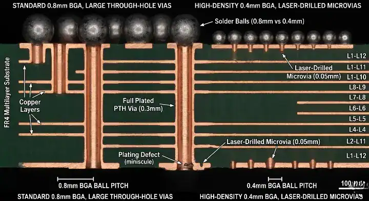
BGA pitch dictates your via strategy, with 0.5mm acting as the definitive tipping point where you must abandon standard through-holes and use HDI technology. When working with a 0.5mm pitch, the minimum viable drill is 6mil with a 10mil pad, leaving only a 2mil annular ring—forcing the use of VIPPO (via-in-pad plated over) or staggered microvias. Implementing microvia optimization techniques at these pitches prevents costly fabrication failures.
The 0.5mm Tipping Point
A user on the SierraConnect Forum asked: “Is My HDI Via Strategy Correct for .5mm FBGA? Should I use stacked vias or via-in-pad?”
For a 0.5mm FBGA, standard dog-bone fanouts become manufacturing nightmares. You must transition to plated in-pad microvias (VIPPO) or staggered microvias. Furthermore, at 0.5mm pitch, you should never attempt to route traces between pads unless your fabrication partner can reliably produce sub-4mil traces with high yield.
Managing 0.4mm BGA Breakout
Another engineer on the forum questioned: “Currently, I have a 2-2-2 stackup with uVias and buried vias. Based on my board thickness, I am using a uVia with a 6mil hole and 10mil pad. Is this strategy reasonable for a 0.4mm pitch BGA?”
Yes, this is the industry-standard approach. For a 0.4mm pitch BGA, HDI is mandatory because dog-bone fanouts are physically impossible. A 2-2-2 stackup with a 6mil microvia hole and 10mil pad is a highly reliable configuration. To execute the Z-axis fanout, route the outer row of pins on Layer 1, the second row on Layer 2 via microvias, and so forth.
| BGA Pitch | Recommended Via Strategy | HDI Requirement |
|---|---|---|
| 1.0mm | Standard Through-Hole | Not Required |
| 0.8mm | Dog-bone Fanout | Not Required |
| 0.65mm | Sub-lamination / Blind Vias | Optional |
| 0.5mm | VIPPO / Staggered Microvias | Required |
| 0.4mm | 2-2-2 Stackup / Microvias | Mandatory |
| 0.3mm | ELIC (Every Layer Interconnect) | Mandatory |
Analysis Guide: If your design features components at 0.65mm pitch or larger, stick to standard multi-layer. If you drop to 0.5mm or below, you must factor HDI costs into your budget immediately.
Bottom line: The moment your BOM includes a component with a 0.5mm pitch or tighter, standard PCB fabrication is no longer viable, and you must switch to a microvia-based HDI stackup.
3. When Does Routing Congestion Force You to Switch to HDI?
Routing congestion forces a switch to HDI when you have components with over 300 pins and cannot successfully complete escape routing within the first 4 internal layers using standard vias. Standard through-holes consume space on every single layer of the board, creating massive routing blockages on lower layers. Microvias, on the other hand, only penetrate 1-2 layers, freeing up critical routing channels directly beneath dense components.
Recognizing the Routing Wall
You hit the routing wall when your via density prevents traces from passing through component footprints. Routing channel exhaustion is the state where the physical distance between through-hole vias is smaller than your minimum trace/space requirements. When this happens, adding more standard layers only makes the problem worse, as the through-holes will continue to eat up space on the newly added layers.
The QueenEMS Engineering Perspective
We frequently see customers misdiagnose routing congestion.
- The Problem: A customer recently submitted a 12-layer standard board design trying to route a high-pin-count FPGA. They suffered from severe crosstalk because their through-holes destroyed the ground planes.
- Our Solution: We redesigned their stackup using a 1+N+1 HDI architecture.
- The Result: By switching to blind microvias, we opened up massive routing channels, reducing the board to 8 layers, dropping overall thickness by 30%, and completely eliminating the crosstalk issues.
Bottom line: Stop adding standard layers when you run out of routing room; if through-holes are causing the blockage, switching to blind microvias is the only geometric solution.
4. Can Layer Count Reduction Justify the HDI PCB Cost Premium?
Yes, reducing your layer count by 40–50% frequently justifies the HDI cost premium, turning an expensive technology into a net-cost saver. While the per-layer cost of an HDI board is 1.5 to 3 times higher than a standard board, dropping a design from 12 standard layers down to 6 HDI layers typically results in a 15–25% reduction in total bare board costs. Reviewing a detailed HDI vs standard PCB cost comparison is critical before finalizing your BOM.
The Math Behind the Savings
Standard FR4 1oz multi-layer boards have a high first-pass yield, but once you exceed 10 layers, the material costs and lamination risks increase sharply.
- Sequential lamination is the process of pressing a PCB multiple times to create buried and blind vias.
- While sequential lamination adds $0.15–$0.30 per square inch in manufacturing costs, eliminating 4-6 layers of FR4 material and copper foil often completely offsets this fee.
Break-Even Analysis
| Stackup Type | Layer Count | Relative Cost Factor | Yield Risk |
|---|---|---|---|
| Standard Through-Hole | 6 Layers | 1.0x (Baseline) | Low |
| Standard Through-Hole | 12 Layers | 2.5x | Medium |
| 1+N+1 HDI | 8 Layers | 2.2x | Low-Medium |
| 2+N+2 HDI | 6 Layers | 2.1x | Medium |
Analysis Guide: Choose standard fabrication if your design routes cleanly in 8 layers or less. Choose HDI if standard routing forces you past 10 layers, as the layer reduction will offset the HDI premium.
Bottom line: Never compare HDI and standard boards on a per-layer basis; calculate your total landed cost based on the reduced layer count that microvias enable.
5. How Do High-Speed Signal Integrity Requirements Trigger HDI Adoption?

High-speed signal integrity requirements trigger HDI adoption when data rates exceed 10Gbps, because microvias improve signal integrity by 15–20% compared to standard through-holes. At speeds seen in DDR5, PCIe Gen5, and USB4, the parasitic capacitance and inductance generated by standard vias severely degrade the signal. HDI allows for tighter impedance control (±5% vs standard ±10%) and significantly shorter signal paths.
Solving Eye Diagram Failures
A frustrated engineer on an EEVBlog forum stated: “I’m designing a DDR4/DDR5 board and have eye diagram failures with my current 8-layer stackup. Do I need to switch to HDI?”
The short answer is yes. A via stub is the unused portion of a through-hole via that hangs below the signal trace, acting as an antenna that reflects high-speed signals. For data rates ≥10Gbps (like 112G PAM4 or DDR5), these stubs destroy your eye diagram. Microvias eliminate stubs entirely by stopping exactly at the target layer, instantly cleaning up the return path.
The QueenEMS Engineering Perspective
Signal integrity requires physical precision that standard drilling cannot achieve.
- The Problem: An AI server startup was failing FCC emissions testing because their PCIe Gen5 traces were routed using standard through-holes with back-drilling, leaving tiny but impactful stubs.
- Our Solution: We transitioned their high-speed nets to a staggered microvia HDI design, completely eliminating the need for back-drilling.
- The Result: The signal path parasitic inductance dropped by 18%, the eye diagram opened up by 30mV, and the board passed compliance testing on the first run.
Bottom line: If your design features data rates above 10Gbps, standard through-hole vias will act as signal-destroying antennas; HDI microvias are mandatory for clean signal integrity.
6. When Is Standard Multilayer PCB Still the Better Choice?
A standard multilayer PCB is the better choice when your smallest BGA pitch is ≥0.8mm, your high-speed signals are under 5GHz, and you have ample board space (>50cm²). HDI is not a magic bullet; it is an expensive solution to specific physical constraints. If you can complete your routing on a 4-to-8 layer through-hole board and meet your impedance targets, an optimized standard build will always be more cost-effective and faster to produce.
Avoiding the Overkill Trap
Engineers frequently ask on EEVBlog: “Is HDI overkill for our design? We have one 0.65mm BGA but the rest is regular components. Don’t want to overpay.”
For a single 0.65mm to 0.8mm BGA, HDI is absolutely overkill. You can successfully escape route this component using a standard build with sub-lamination blind vias. You do not need laser-drilled microvias for this pitch. Refer to a multilayer PCB stackup design guide to learn how to optimize blind vias without triggering HDI pricing.
The Anti-HDI Checklist
You should NOT use HDI if your project matches these conditions:
- You are in an early prototype phase and board size is not yet restricted.
- Your component count is low, and your BGA pitches are 0.8mm or wider.
- Your factory quotes a standard 6L board at $2 per unit, while a 1+N+1 HDI 6L board quotes at $5 per unit.
- A single fine-pitch component can be routed using standard sub-lamination without adding overall layers.
Bottom line: Do not force an HDI stackup onto a design that doesn’t need it; if a standard 6-layer board meets your routing and signal needs, enjoy the cheaper manufacturing costs.
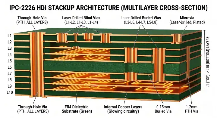
7. What IPC-2226 Type Should You Pick for When to Use HDI PCB Decisions?
When deciding to use HDI, you must select the correct IPC-2226 Type: choose Type I for a single layer of microvias (1+N+1), Type II when you need buried vias alongside microvias, and Type III for dense designs requiring multiple staggered or stacked microvia layers (2+N+2 or higher). Your choice directly impacts your sequential lamination cycles, which drives both cost and fabrication lead times.
Understanding Aspect Ratios and Stackups
Before choosing a type, you must respect the microvia aspect ratio. The microvia aspect ratio is the ratio of the via depth to its diameter. According to IPC-6016, this ratio must remain ≤1:1 to ensure reliable copper plating. If your dielectric layer is too thick, your laser drill hole must be wider, which defeats the purpose of fine-pitch routing.
Furthermore, when deciding between stacked vs. staggered microvias, remember that staggered vias are highly reliable, whereas stacked microvias should generally be limited to 2 layers due to the immense thermal stress they endure during reflow.
| IPC-2226 Type | Architecture | Best For… | Cost Level |
|---|---|---|---|
| Type I | 1+N+1 (No buried vias) | Simple consumer electronics, ≤0.65mm BGA | Lowest HDI Premium |
| Type II | 1+N+1 (With buried vias) | Smartphones, tablets, via-in-pad needs | Moderate |
| Type III | 2+N+2 or ≥3+N+3 | Complex servers, ≤0.4mm BGA, dense routing | High |
| ELIC | Every Layer Interconnect | Ultra-dense wearables, smartphones | Highest |
Analysis Guide: Start your HDI design by attempting a Type I (1+N+1) stackup. Only upgrade to Type II or Type III if you absolutely cannot complete the Z-axis fanout on the outer dielectric layers.
Bottom line: Always default to the simplest IPC-2226 Type I architecture; only accept the manufacturing risks of Type III stacked microvias when your BGA pitch drops to 0.4mm or below.
8. What DFM Mistakes Cause “False HDI Need” in Standard Designs?
Design for Manufacturing (DFM) mistakes cause “false HDI needs” when engineers use unnecessarily wide traces, oversized via capture pads, or poor component placement, artificially exhausting routing channels on standard boards. Hardware teams often assume they need HDI because their layout software flags hundreds of DRC errors, but a thorough DFM review usually reveals that optimizing standard design rules can solve the congestion without adding laser-drilled microvias.
The “False Alarm” Checklist
Factories frequently receive designs that claim to “need” HDI, but actually suffer from poor planning.
- Trace Width: Using 8mil traces for low-current digital signals when the fab house can easily process standard 4mil/4mil rules.
- Via Density: Placing excessive stitching vias or failing to use shared ground vias for bypass capacitors, eating up board space.
- Layer Planning: Failing to assign dedicated orthogonal routing directions for adjacent signal layers, leading to blocked Z-axis transitions.
The QueenEMS Engineering Perspective
We save clients thousands of dollars by identifying false HDI alarms.
- The Problem: A medical device startup submitted a 10-layer design, believing they needed HDI because their autorouter failed to complete escape routing around an STM32 microcontroller.
- Our Solution: We performed a free DFM review, reduced their oversized 14mil via pads to a standard 10mil, and reorganized their decoupling capacitors to share ground vias.
- The Result: The board routed cleanly on a standard 8-layer FR4 stackup, reducing their prototype costs by 60% and cutting lead times by 5 days.
Bottom line: Before committing to expensive HDI manufacturing, have your fabrication partner run a DFM check to ensure your congestion isn’t just the result of oversized standard routing rules.
9. How Much Cost Premium Should You Expect for HDI vs Standard PCBs?
You should expect an HDI cost premium of 1.5 to 3 times the base price of a standard PCB, driven primarily by the required sequential lamination cycles, laser drilling time, and specialized via-filling processes. Every time the board goes through an additional lamination press cycle (e.g., moving from 1+N+1 to 2+N+2), the fabrication time extends, yields drop slightly, and labor costs increase.
Breaking Down the Premium
Sequential lamination is the repetitive process of pressing copper foil and prepreg, drilling, plating, and etching. A standard board goes through the press once. A 2-2-2 HDI board goes through the press three times. This adds an average of 24 to 48 hours to fabrication lead times. Additionally, because microvias are often placed inside component pads (VIPPO), they require specialized epoxy filling and planarization to create a flat soldering surface, adding $0.02–$0.05 per via to your total cost.
| Manufacturing Step | Standard Multilayer Cost | HDI Premium Addition |
|---|---|---|
| Lamination | Single Press (Base Cost) | +30-50% per extra press cycle |
| Drilling | Mechanical only (Base) | +$100-$300 setup for Laser Drill |
| Plating / Filling | Standard hole wall (Base) | +15-20% for Via Filling/Planarization |
| Yield Loss | Minimal | +5-10% buffer built into pricing |
Analysis Guide: If your production volume is under 100 units, the one-time HDI setup costs (NRE) will severely inflate your per-board price. HDI becomes much more economical at volumes above 1,000 units.
Bottom line: The HDI cost premium is inescapable due to laser drilling and sequential pressing; only absorb this cost when the layer reduction or signal integrity benefits offer a clear return on investment.
10. How Do You Validate Your HDI Decision Before Layout Begins?
You validate your HDI decision before layout begins by isolating your most complex component (usually the finest-pitch BGA), placing it on a blank digital canvas with your proposed stackup, and performing a quick escape routing test. If you can cleanly break out all the inner pins of that specific component using standard vias, you do not need HDI. If you cannot, you immediately know you must adjust your stackup architecture before spending weeks routing the rest of the board.
The Pre-Layout Validation Checklist
Do not wait until the board is 90% routed to realize you need microvias. Follow this sequence:
- Check Pitch: Identify the absolute tightest component pitch on your BOM.
- Calculate Drill/Pad: Determine if your fab house’s minimum mechanical drill/pad size fits within that pitch while leaving a safe 4mil web between pads.
- Test Escape: Perform a fanout study on that single component.
- Count Layers: Tally how many layers the escape routing consumed. Does it push your total board thickness out of spec?
By doing this validation on day one, you synchronize your CAD tool’s DRC rules with reality. Attempting to switch a layout from standard through-holes to an HDI 2-2-2 stackup halfway through the design process requires ripping up and re-routing almost everything.
Bottom line: Validate your need for HDI by doing a localized fanout test on your densest BGA on day one; if it fails standard routing, lock in an HDI stackup before routing another trace.
Conclusion
Deciding when to use HDI PCB technology comes down to simple math: component pitch, layer count limits, and data rates. If your BGA drops to 0.5mm, your signal speeds cross 10Gbps, or your standard layer count balloons past 12, it is time to embrace microvias. While HDI carries a higher per-layer cost, the ability to shrink your board footprint, reduce total layers, and eliminate signal-destroying via stubs makes it an incredibly powerful tool for modern hardware.
QueenEMS provides free DFM reviews to help you determine exactly when standard multilayer ends and HDI begins. If you are struggling with a dense layout or failing eye diagrams, contact our PCB engineering team today. We will evaluate your stackup, run a breakout study, and ensure you are choosing the most cost-effective fabrication strategy for your project.
Written by the QueenEMS Engineering Team
FAQs
Can I use a standard PCB stackup for a 0.5mm BGA? No, a 0.5mm pitch requires HDI via-in-pad or staggered microvias. A standard mechanical drill (usually 8mil minimum) with an appropriate pad size will not fit between the pins without violating manufacturing clearances. Switch to a microvia strategy to ensure successful fabrication.
How do I know if my routing congestion requires HDI? Yes, you need HDI if you have exhausted all standard routing channels and cannot escape route a component within 4 internal layers. If adding more through-hole layers only creates more blockage, blind microvias are the only way to free up Z-axis space. Request a stackup review from your manufacturer.
Is it cheaper to use a 12-layer standard board or an 8-layer HDI board? Yes, the 8-layer HDI board is often cheaper in overall cost. While HDI processes cost more per layer, eliminating 4 layers of FR4 material and copper foil usually results in a 15–25% net savings. Always calculate your total landed cost rather than just looking at the technology premium.
Does HDI improve high-speed signal integrity? Yes, HDI improves signal integrity by 15–20% for data rates over 10Gbps. Microvias eliminate the unused via “stubs” found in standard through-holes, removing the parasitic capacitance that causes reflections and eye diagram failures. Switch to HDI for cleaner PCIe Gen5 or DDR5 routing.
What is the maximum reliable microvia aspect ratio? The maximum reliable aspect ratio is 1:1, meaning the laser-drilled hole depth cannot exceed its diameter. Pushing past this limit leads to poor copper plating and field failures. Keep your dielectric layers thin to support smaller microvias.
Upload your files today · Free DFM check before production · Ship worldwide
Get your PCB prototypes in as fast as 24 hours. We handle FR4, Rogers, and Flex up to 60 layers — free prototypes for 2–4 layer boards, no minimum order.
Just upload your Gerber + BOM — we source every part, assemble, and inspect (AOI + X‑Ray) so you don't have to chase suppliers. Boards ship in as fast as 24 hours.