
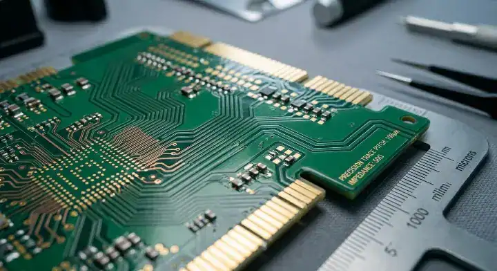
Quick Answer: A controlled impedance PCB strictly regulates the alternating current resistance on high-speed traces, costing 5% to 15% more than standard boards due to specialized TDR testing. A typical 50Ω microstrip trace on a 0.1mm prepreg layer requires a 0.15mm trace width, and shrinking your manufacturing tolerance from ±10% to ±5% will increase your unit price by up to 20%.
Key takeaways:
- Standard FR4 introduces a ±10% Dk variance; high-frequency designs require Rogers materials with ±1.5% tolerances.
- Mixed stackups (Rogers + FR4) reduce material expenses by 40% to 60%.
- Etch compensation prevents the physical trace from narrowing and spiking the final impedance value.
- Time-Domain Reflectometer (TDR) test coupons physically prove the manufacturer met your specifications.
Table of Contents
- What Is Controlled Impedance and When Does Your PCB Need It?
- How Do Trace Geometry and Stackup Affect PCB Impedance?
- How Do You Calculate Impedance for Microstrip, Stripline, and Coplanar Waveguide?
- What Materials Should You Choose for Impedance-Controlled Boards?
- How Should You Specify Impedance Requirements to Your PCB Manufacturer?
- How Do Manufacturers Achieve and Verify Controlled Impedance?
- What Are the Most Common Impedance Control Failures and How Do You Prevent Them?
- How Much Does Controlled Impedance PCB Fabrication Cost?
- FAQ
You calculate a perfect 50Ω trace in your EDA tool, send the files out, but the physical board returns measuring 58Ω, causing massive data loss on your PCIe interface. That mismatch forces a total layout redesign, wasting thousands of dollars and weeks of engineering time. After processing 4,000+ controlled impedance PCB orders last year, we watch hardware teams repeat the exact same specification errors. Here is exactly how physical manufacturing alters your mathematical models and how to lock down your signal integrity.
What Is Controlled Impedance and When Does Your PCB Need It?
Controlled impedance limits the alternating current resistance on high-speed traces to specific targets like 50Ω single-ended or 100Ω differential. It is required whenever signal rise times drop below 1 nanosecond or operating frequencies exceed 300MHz to prevent catastrophic signal reflection. Unlike simple DC resistance measured in ohms, impedance accounts for inductance and capacitance changing at high frequencies.
When digital signals travel down a trace, they expect a uniform electrical environment. If the trace width suddenly changes or the dielectric layer thins out, the impedance shifts. This shift causes the signal to bounce back towards the source, creating interference known as ringing. You must implement strict controls on both the design side and the manufacturing floor to maintain a stable transmission line.
Now, here’s the part that surprises most customers… many designers attempt to run fast USB 3.0 lines on standard boards without specifying impedance, incorrectly assuming short trace lengths will save them.
- Single-ended impedance: Typically 50Ω, used for RF antennas and single high-speed signals.
- Differential impedance: Typically 85Ω to 100Ω, used for paired signals like USB, HDMI, and PCIe to cancel out noise.
- Frequency threshold: Any trace acting as a transmission line (length > 1/10th of the wavelength) needs control.
Common High-Speed Interface Requirements
Different digital protocols demand entirely different target values.
| Interface Name | Impedance Type | Target Value | Standard Tolerance | Typical Trace Width Range |
|---|---|---|---|---|
| USB 2.0 | Differential | 90Ω | ±10% | 0.10mm – 0.15mm |
| USB 3.0 / 3.1 | Differential | 90Ω | ±10% | 0.10mm – 0.15mm |
| HDMI | Differential | 100Ω | ±10% | 0.12mm – 0.18mm |
| PCIe (Gen 3/4) | Differential | 85Ω | ±10% (often ±5%) | 0.10mm – 0.12mm |
| RF Antennas | Single-ended | 50Ω | ±5% | 0.20mm – 0.35mm |
Matching these exact targets dictates whether your device passes FCC emission testing or fails instantly.
Bottom line: If your board features USB, HDMI, PCIe, or any RF module, you must explicitly declare controlled impedance targets to prevent data packet loss and signal reflection.
How Do Trace Geometry and Stackup Affect PCB Impedance?
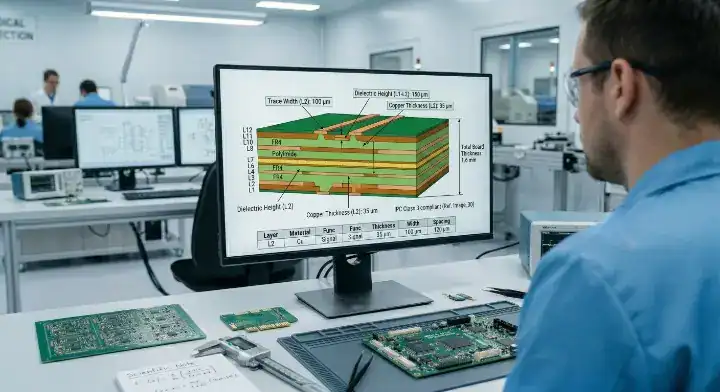
Four physical parameters control PCB impedance: trace width (W), dielectric thickness (H), copper thickness (T), and the dielectric constant (Dk). Increasing the trace width decreases the final impedance, while increasing the dielectric thickness between the trace and the reference plane raises it significantly.Before finalizing your trace width for impedance control, verify the width can safely handle the required current using our PCB Trace Width Calculator.
Every tiny adjustment in your EDA stackup manager alters the mathematical outcome. If you use a heavy 2oz copper thickness for power delivery on the same layer as your high-speed signals, the added copper height (T) will drop your impedance, forcing you to shrink the trace width to compensate. The dielectric constant (Dk) represents how much the FR4 or Rogers material slows down the electrical signal.
The real question is… do you control the impedance, or do you let the manufacturer control the dielectric?
- Trace Width (W): Inversely proportional. Wider traces = lower impedance.
- Dielectric Height (H): Directly proportional. Thicker FR4 = higher impedance.
- Copper Thickness (T): Inversely proportional. Thicker copper = lower impedance.
- Dielectric Constant (Dk): Inversely proportional. Higher Dk = lower impedance.
Parameter Impact on Signal Integrity
Understanding which variable to tweak saves hours of redesign work.
| Physical Parameter | Action Taken | Resulting Impedance Shift | Manufacturing Difficulty |
|---|---|---|---|
| Trace Width (W) | Increase width | Decreases | Easy (Controlled by laser imaging) |
| Dielectric Height (H) | Increase thickness | Increases | Hard (Depends on prepreg resin flow) |
| Copper Thickness (T) | Increase weight | Decreases slightly | Medium (Depends on plating process) |
| Dielectric Constant (Dk) | Switch to lower Dk | Increases | Hard (Requires totally different material) |
Locking in your base material first prevents you from chasing impossible geometry targets later.
Bottom line: Fix your dielectric material and desired copper weight first, as these two variables dictate 90% of your final trace width calculations.
How Do You Calculate Impedance for Microstrip, Stripline, and Coplanar Waveguide?
Calculating impedance requires choosing a physical structure: a microstrip resting on the outer layer, a stripline buried between two solid ground planes, or a coplanar waveguide with side-grounding copper. A standard 50Ω microstrip built on a 0.1mm prepreg typically demands a 0.15mm trace width, but moving that exact same trace to an internal stripline requires shrinking the width drastically to maintain 50Ω.
A microstrip offers fast signal propagation because one side is exposed to air (which has a Dk of 1.0). A stripline completely encases the trace in FR4, slowing the signal down but providing perfect EMI shielding. A coplanar waveguide (CPW) places grounding copper directly next to the trace on the same layer, providing extreme isolation for RF signals without needing a thick substrate.
You can use a standard PCB impedance calculator for initial estimates, but physical manufacturing always introduces variables that basic formulas ignore.
Here’s where it gets real… simplified online calculators assume perfect rectangular traces, but actual etched traces are trapezoidal.
- Microstrip: Outer layers. Fast speeds, easy to troubleshoot, poor EMI shielding.
- Stripline: Inner layers. Slower speeds, excellent EMI shielding, requires vias to access.
- Coplanar Waveguide: Any layer. Best isolation, used heavily in high-frequency RF.
Transmission Line Structure Comparison
Your layout density dictates which structure you physically have room to build.
| Structure Type | Reference Planes | EMI Shielding | Impedance Consistency | Typical Application |
|---|---|---|---|---|
| Microstrip | 1 (Below) | Poor | Good | Surface components, short PCIe runs |
| Stripline | 2 (Above & Below) | Excellent | Very High | Dense internal routing, sensitive data |
| Coplanar Waveguide | 1 (Below) + Side ground | Excellent | Extreme | Wi-Fi antennas, radar, 5G RF modules |
Using a 2D field solver program provides far more accurate calculations than algebraic formulas.
Bottom line: Use internal stripline configurations for sensitive high-speed signals to guarantee EMI shielding, and reserve microstrips for surface-level routing where troubleshooting access is required.
What Materials Should You Choose for Impedance-Controlled Boards?
Standard FR4 exhibits a Dk tolerance of ±10%, causing impedance variations across different manufacturing batches, whereas Rogers RO4350B maintains a strict ±1.5% Dk tolerance for high-frequency stability above 3GHz. If you try to run a 10Gbps signal through standard FR4, the high dissipation factor (Df) will absorb the signal, converting your data into pure heat.
Hardware engineers on forums constantly debate the cost of upgrading. Rogers material costs five to ten times more than FR4. To solve this, smart designers use a mixed stackup—placing a Rogers layer on top for the RF signals, and standard FR4 material properties for the internal digital logic. This hybrid approach saves 40% to 60% in material expenses.
However, mixing materials creates a massive Coefficient of Thermal Expansion (CTE) mismatch. If the FR4 expands faster than the Rogers core during the pressing cycle, the board warps. You must use high-Tg FR4 (150°C+) to mitigate this physical stress.
But here’s what most guides won’t tell you… using a single ply of 1080 glass weave prepreg creates the “glass weave effect,” where the signal physically bounces off the glass bundles, destroying your impedance matching on long runs.
- FR4 Dk varies by batch and by the specific resin-to-glass ratio.
- Rogers materials provide extreme consistency but require special drill bits.
- Avoid using single-ply low-resin prepregs (like 1080) for high-speed differential pairs.
Material Dk/Df Properties and Applicability
Choosing the right substrate prevents total signal loss at high frequencies.
| Material Type | Typical Dk Value | Dk Tolerance | Dissipation Factor (Df) | Usable Frequency | Relative Cost |
|---|---|---|---|---|---|
| Standard FR4 | 4.2 – 4.6 | ±10% | 0.020 | < 3 GHz | Baseline (1x) |
| High-Tg FR4 | 4.2 – 4.5 | ±8% | 0.015 | < 5 GHz | 1.2x |
| Rogers RO4350B | 3.48 | ±1.5% | 0.0037 | Up to 40 GHz | 5x – 8x |
| Teflon (PTFE) | 2.1 – 2.9 | ±1.0% | 0.0010 | > 40 GHz | Extreme (10x+) |
If you run a mixed stackup, you must calculate the impedance for each layer separately, as the Dk values will clash.
Bottom line: Stick to high-Tg FR4 for digital signals under 3GHz to save money, but immediately upgrade your RF layers to Rogers RO4350B to prevent severe signal degradation and batch-to-batch inconsistency.
How Should You Specify Impedance Requirements to Your PCB Manufacturer?
Your fabrication notes must explicitly list the target impedance, trace width, specific copper layer, structure type, and acceptable tolerance (typically ±10%). Vague requests like “match 50-ohm impedance” force manufacturers to guess your intended reference planes, adding 2 to 3 days to your quoting time while they email you for clarification.
80% of incoming designs contain vague impedance notes that lack exact trace spacing for differential pairs. We built a standardized stackup template that forces designers to declare trace width and spacing upfront, cutting our pre-production engineering holds from 48 hours down to absolute zero. If you do not tell the CAM engineer which exact traces need control, they will not adjust them during the tooling phase.
You must also demand a TDR test report in your fab notes. If you do not explicitly request this documentation, lower-end brokers will skip the testing entirely to save money, leaving you with no proof that the physical board actually hits the required targets.
So what does this actually mean for your budget? Clear documentation prevents the factory from applying unnecessary strict tolerances to power traces, saving you money.
- Never mix different impedance targets on the exact same trace width on a single layer.
- Always define the spacing for differential pairs, not just the single trace width.
- Include a full stackup drawing showing core and prepreg thicknesses.
Impedance Control Spec Sheet Template
Copy this exact format into your fabrication drawing notes to eliminate factory confusion.
| Layer | Trace Type | Target Impedance (Z) | Trace Width (W) | Spacing (S) | Reference Dielectric | Tolerance |
|---|---|---|---|---|---|---|
| L1 (Top) | Single-ended | 50Ω | 0.15mm | N/A | L1 to L2 Prepreg | ±10% |
| L1 (Top) | Differential | 90Ω | 0.12mm | 0.15mm | L1 to L2 Prepreg | ±10% |
| L3 (Inner) | Stripline | 50Ω | 0.10mm | N/A | L2 to L4 Core/PP | ±5% |
| L8 (Bot) | Coplanar | 50Ω | 0.20mm | 0.20mm gap | L7 to L8 Prepreg | ±10% |
Using this table prevents the manufacturer from guessing your design intent.
Bottom line: Provide a complete impedance table in your Gerber fab notes detailing the exact trace width, spacing, and target layer to eliminate pre-production delays and ensure accurate etching.
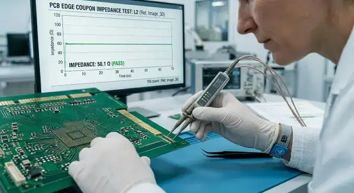
How Do Manufacturers Achieve and Verify Controlled Impedance?

PCB manufacturers achieve precise impedance by applying etch compensation to your trace widths and calculating the actual pressed dielectric thickness based on copper density. They verify the final results by attaching a test coupon to the manufacturing panel perimeter and measuring it with a Polar Instruments Time-Domain Reflectometer (TDR).
Over 60% of prototype boards fail TDR tests at generic factories because they ignore the prepreg resin flow effect. When a board is pressed under high heat, the liquid resin flows into the empty spaces between the copper traces. If a layer lacks copper, more resin flows out, making the final dielectric layer thinner than the data sheet states. We implemented mandatory CAM-level etch compensation and press-out thickness modeling, allowing us to hit a tight ±5% impedance tolerance with a 99.7% first-pass yield rate.
Etch compensation is critical because the chemical bath eats copper from the sides as well as the top, turning a perfect rectangular trace into a trapezoid. If the CAM engineer does not artificially widen your trace on the film to compensate for this undercut, your physical trace ends up too narrow, and your impedance spikes.
Want the honest answer? The manufacturer cannot test the actual traces on your board; they test a replicated coupon located on the panel’s breakaway edge.
- Etch Compensation: Widening the Gerber trace slightly to account for chemical side-etching.
- Press-Out Calculation: Adjusting expected dielectric height based on actual copper area.
- TDR Testing: Sending a fast step pulse into the test coupon and measuring the reflected wave to calculate exact impedance.
Manufacturing Adjustments vs Impact
A quality multilayer PCB manufacturer changes your files intentionally to save the final product.
| Factory Process | What the Manufacturer Changes | Why It Prevents Failure |
|---|---|---|
| Etch Compensation | Increases trace width on the photo-tool by 0.5 to 1 mil. | Offsets the chemical undercut, keeping the final physical width accurate. |
| Press-Out Modeling | Selects a slightly thicker prepreg style. | Compensates for resin flowing into sparse copper areas during lamination. |
| Coupon Generation | Adds a test trace to the panel waste rail. | Allows physical TDR testing without destroying your actual finished board. |
| Impedance Tuning | Alters your requested trace width by up to 10%. | Forces the physical board to hit the 50Ω target despite material variances. |
If a factory refuses to provide a Polar TDR report, they likely skipped these engineering steps.
Bottom line: Never accept an impedance-controlled batch without demanding the physical Polar TDR test report generated directly from your specific manufacturing panel.
What Are the Most Common Impedance Control Failures and How Do You Prevent Them?
The most common impedance failure occurs when engineers simulate 50Ω using a generic Dk value, but the physical board measures 55Ω because prepreg resin flow shrunk the dielectric thickness. Failing to model copper etching and mixing multiple impedance targets on a single layer also severely warp the final physical measurements, causing massive forum debates between designers and fabricators.
Many engineers complain their 10Gbps signals degrade rapidly because their previous supplier ignored copper profile roughness. Standard copper foil has a rough “tooth” to help it stick to the FR4. At high frequencies, the “skin effect” forces the signal to travel strictly along this bumpy surface, increasing the effective Dk and dropping the impedance. We standardized the use of low-profile (LP) copper foil on all high-speed RF batches, completely eliminating signal loss variations caused by rough copper profiles.
Another massive trap is assigning a 50Ω target to a 0.15mm trace, and a 90Ω target to a different 0.15mm trace on the exact same layer. The CAM engineer cannot apply different etch compensations to the identical widths on the same plane. You must use unique trace widths for unique targets.
Here’s where it gets real… if you use a generic online calculator, you are guaranteed to miss your target by at least 10% on the first run.
- Dk Mismatch: Generic CAD Dk values never match the specific factory’s Shengyi or ITEQ material data sheets.
- Resin Starvation: Large copper voids cause prepreg to thin out, drastically raising impedance.
- Skin Effect: High-frequency signals travel further on rough copper, skewing the math.
Impedance Failures and Prevention Checklist
Stop fighting the factory and start designing for the physical reality of lamination.
| Common Failure Mode | Root Cause | How to Prevent It in Design |
|---|---|---|
| Target missed by +5Ω | Prepreg pressed thinner than expected. | Ask factory for “press-out” thickness, not nominal thickness. |
| Target missed by +8Ω | Trace narrowed due to chemical undercut. | Allow the factory to apply ±10% trace width adjustments. |
| High-frequency signal loss | Copper surface roughness altered effective Dk. | Specify Low-Profile (LP) or Very-Low-Profile (VLP) copper foil. |
| Factory halts production | Multiple impedance targets share one trace width. | Assign unique widths (e.g., 0.15mm for 50Ω, 0.14mm for 90Ω). |
Relying on a 2D field solver program inside Altium or Cadence is mandatory for modern stackups.
Bottom line: Always request your manufacturer’s specific, pre-calculated stackup parameters and material Dk values before you begin routing to prevent post-fabrication impedance mismatches.
How Much Does Controlled Impedance PCB Fabrication Cost?
Adding standard ±10% controlled impedance testing typically increases your total PCB fabrication cost by 5% to 15% due to added CAM engineering time and TDR test coupon generation. Demanding a strict ±5% tolerance requires extreme laser etching precision and drops panel yields, driving prices up by an additional 15% to 20%.
The cost jump is not just a markup for the testing equipment. Hitting a tight tolerance requires the factory to buy higher-grade materials with tighter Dk consistency. They must also slow down their chemical etching lines to prevent excessive trace undercutting. If a panel fails the TDR test at the end of the line, the entire batch goes into the trash, meaning the factory bakes that high scrap risk directly into your initial quote.
Now, here’s the part that surprises most customers… you are paying for the engineering time to adjust your flawed stackups just as much as the physical copper.
- CAM Engineering: Takes hours to calculate press-out thickness and etch compensations.
- TDR Testing: Requires specialized Polar equipment and trained technicians to read the waveforms.
- Scrap Rate: Tighter tolerances (±5%) drastically increase the number of rejected panels.
Cost Impact Breakdown
Every constraint you add to the fab notes multiplies the final invoice.
| Impedance Requirement | Estimated Cost Premium | Primary Driver of the Price Increase |
|---|---|---|
| No Control | Baseline ($0) | Standard high-volume pooling processes. |
| Impedance Control (±10%) | + 5% to 15% | CAM adjustments, TDR coupons, and testing labor. |
| High Precision Control (±5%) | + 20% to 35% | Premium materials, slower etching, and high scrap rates. |
| Rogers Material Upgrade | + 400% to 800% | Exotic PTFE/ceramic substrates for high frequency. |
Do not demand ±5% unless your specific protocol (like PCIe Gen 4) legally mandates it.
Bottom line: Specify the standard ±10% tolerance to keep your fabrication budget low, and only mandate a strict ±5% tolerance for highly sensitive RF or ultra-high-speed digital applications.
FAQ
Can I use a standard PCB stackup for a controlled impedance design? No. Standard pooling stackups use generic prepreg materials where the exact thickness and dielectric constant (Dk) vary wildly between batches. To control impedance, you must use a custom stackup where the manufacturer guarantees the specific material brands, glass weave styles, and pressed thicknesses. Upload your BOM to us to receive a verified custom stackup tailored to your exact trace geometry.
What is the difference between controlling impedance and controlling dielectric? Controlling dielectric means you tell the factory to press the boards to an exact thickness, and you accept whatever final impedance results from your unadjusted trace widths. Controlling impedance means you tell the factory the target ohm value, and you allow them to slightly alter your trace widths and dielectric thicknesses to hit that specific electrical target. Get a transparent quote within 24 hours to see how we manage both methods.
Does copper surface roughness actually impact impedance? Yes. At high frequencies (typically above 3GHz), the “skin effect” forces the electrical signal to travel along the outer surface of the copper trace. If the copper has a rough profile to adhere better to the FR4, the signal path becomes physically longer, which increases the effective dielectric constant and alters the impedance. Request a free first-article inspection on your first order to verify your high-speed signal integrity.
Conclusion
Mastering controlled impedance shouldn’t feel like chasing a moving target — now you have the exact formulas and material knowledge to back your design decisions. You came here trying to understand why your simulated 50Ω traces kept failing physical tests, and now you know exactly how prepreg resin flow, chemical etching undercuts, and generic Dk values alter your mathematical models.
At QueenEMS, we eliminate the guesswork from high-speed signal integrity. We provide ±5% impedance tolerances, run mandatory Polar Instruments TDR testing on every single batch, and pre-adjust your trace widths during the CAM engineering phase so you never fail a final test. We even offer free 2-4 layer FR4 prototypes for new customers to prove our stackup consistency risk-free.
We believe every hardware team deserves a manufacturing partner who understands physical RF realities, not one who just blindly prints flawed files. Contact us today to lock down your high-speed board with a fully verified stackup and transparent quote.
Written by the QueenEMS Engineering Team
Upload your files today · Free DFM check before production · Ship worldwide
Get your PCB prototypes in as fast as 24 hours. We handle FR4, Rogers, and Flex up to 60 layers — free prototypes for 2–4 layer boards, no minimum order.
Just upload your Gerber + BOM — we source every part, assemble, and inspect (AOI + X‑Ray) so you don't have to chase suppliers. Boards ship in as fast as 24 hours.