PCB fabrication · Shenzhen, China
PCB Manufacturing: 1–100 Layer Boards Built in Our Shenzhen Factory
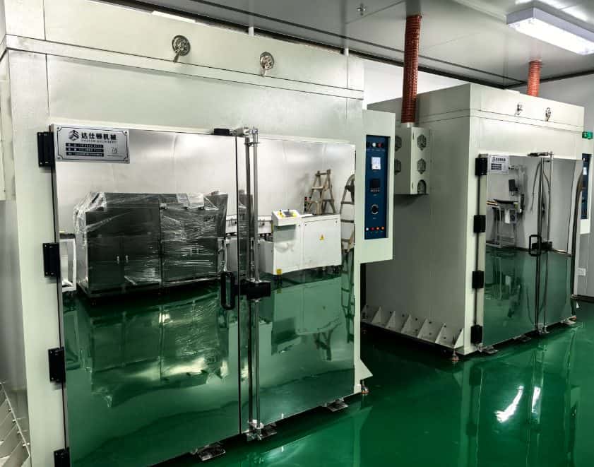
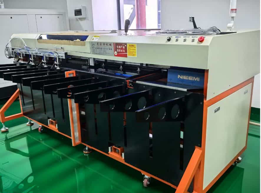
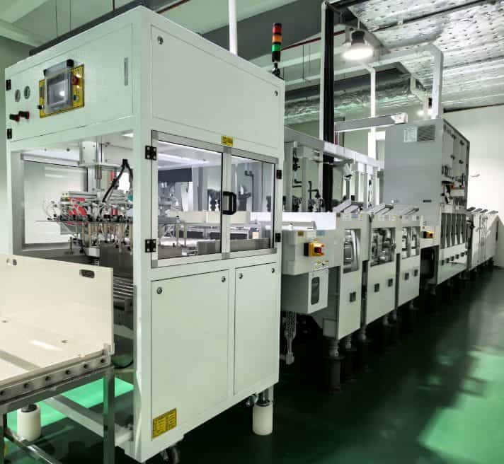
Queen EMS fabricates rigid, HDI, flex, rigid-flex, ceramic and metal core PCBs in our own 30,000 m² factory in Shenzhen for engineering teams in North America, Europe and Asia. Your quote states the material, copper weight, finish and IPC class before production starts.
Buying PCBs overseas
Lower Board Cost Without Guessing at Quality
Most problems with an offshore PCB order come from what was never written down: a laminate swapped for a cheaper equivalent, a finish thinner than expected, or a lead time that was only an estimate.
- Your quote names the laminate, copper weight, surface finish and IPC class we will build to.
- Reference lead times are published by layer count and board area, and your quote confirms the ship date.
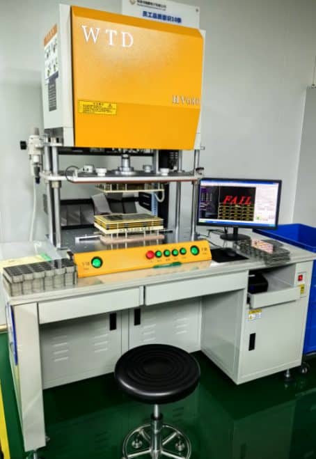
- Every bare board is 100% electrically tested, and ENIG thickness is measured by XRF on every lot, with readings available on request.
Capability index
PCB Fabrication Capabilities, 1 to 100 Layers
| Parameter | Capability | Why it matters |
|---|---|---|
| Layer count | Standard up to 24 layers; advanced up to 100 layers | Covers simple controllers through dense backplanes. See multilayer PCB manufacturing. |
| Board thickness | 0.15–10.0 mm | Thin boards for wearables; thick boards for backplanes and press-fit connectors. |
| Max panel size | 22.5″ × 48″ (572 × 1219 mm) | Long boards for LED, power and industrial panels. See large format PCB. |
| Min line / space | 3/3 mil (75 µm); 6/8 mil at 3 oz; 9/14 mil at 6 oz+ | Sets routing density, and how copper weight limits it. |
| Min mechanical drill | 0.10 mm (4 mil) | Sets how tightly you can fan out through-hole vias. |
| Laser microvia | 0.075 mm (3 mil) | Enables HDI fan-out under fine-pitch BGAs. See HDI PCB. |
| Hole position accuracy | ±0.025 mm | Keeps annular rings intact on dense drill patterns. |
| Aspect ratio | Up to 20:1 | How thick a board can be for a given via size. |
| Min annular ring / mask dam | 3 mil | Pad reliability and solder bridging between fine-pitch pads. |
| Impedance control | ±5%, verified by TDR | USB, PCIe, DDR and RF lines. Check traces with our impedance calculator. |
| Copper weight | Inner 0.5–12 oz; outer 0.5–28 oz; Class 3 hole wall ≥25 µm | Heavy copper for power stages. See heavy copper PCB. |
| Via treatment | Resin plugging; filled & capped via-in-pad (IPC-4761 Type VII) | Vias directly in BGA pads. Read via tenting vs plugging vs filling. |
| Flex / rigid-flex | Flex 1–8 layers; rigid-flex 4–20 layers | See flexible PCB manufacturing. |
| Surface finish | ENIG, ENEPIG, OSP, HASL; hard gold fingers | Pick by pad pitch, shelf life and assembly method. |
| Solder mask | Green, black, blue, red, white, matte | Color has no effect on electrical performance; matte reduces glare for optical inspection. |
| Acceptance standard | IPC-6012 / IPC-A-600, Class 2 or 3 | Defines the plating, annular ring and void limits your board is inspected to. |
These are capability limits, not defaults for every combination. The upper limits are available for prototypes and engineering builds; for production volumes we confirm them case by case. Send your files for a free DFM check and we will flag any feature outside the limits before quoting.
12 board types
PCB Types We Fabricate
Each board type has its own page with detailed capabilities, materials and design rules.
Multilayer PCB
Standard builds to 24 layers, advanced builds to 100, with controlled impedance.
View capabilities →HDI PCB
4–32 layers, 1+N+1 to any-layer (ELIC), stacked and staggered microvias.
View capabilities →Flex & Rigid-Flex
Flex 1–8 layers and rigid-flex 4–20 layers for compact or moving assemblies.
View capabilities →Ceramic PCB
Alumina, AlN and Si3N4 by DBC, DPC, AMB, HTCC and LTCC.
View capabilities →Metal Core PCB
Aluminum and copper base boards for heat spreading.
View capabilities →LED PCB
Boards for lighting modules, drivers and long LED strips.
View capabilities →Heavy Copper PCB
Outer copper up to 28 oz for power and motor drives.
View capabilities →RF & Microwave PCB
Rogers and hybrid stack-ups for antennas, radar and telecom.
View capabilities →BT Substrate PCB
2–16 layer BT resin boards for IC packaging, radar and wireless modules.
View capabilities →Embedded Components
Passive components buried inside the stack-up.
View capabilities →Large Format PCB
Panels up to 22.5″ × 48″ for LED, power and industrial boards.
View capabilities →Rapid Prototyping
Expedited builds for EVT and engineering samples.
View capabilities →Which board type fits your design?
| If your design needs | Start with | Typical use |
|---|---|---|
| Dense BGA fan-out in a small area | HDI PCB | Wearables, compute modules, cameras |
| Many signal and power layers | Multilayer PCB | Industrial control, networking, servers |
| A board that bends or folds | Flex / rigid-flex | Wearables, medical probes, cameras |
| High heat flux or high-voltage isolation | Ceramic PCB | Power modules, laser and LED packages |
| Low-cost heat spreading | Metal core PCB | LED lighting, power supplies |
| High current paths | Heavy copper PCB | Motor drives, battery systems |
| Low signal loss above a few GHz | RF & microwave PCB | Antennas, radar, 5G radios |
Not sure? Compare laminates with our PCB material selector or read the PCB materials guide.
Process
From Gerber to Shipped Board
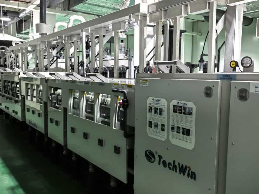
Before anything is built, CAM engineers check your Gerber or ODB++ data, drill files and stack-up notes against our limits. Panels are built to the panel drawing you supply. Then the board moves through our own lines:
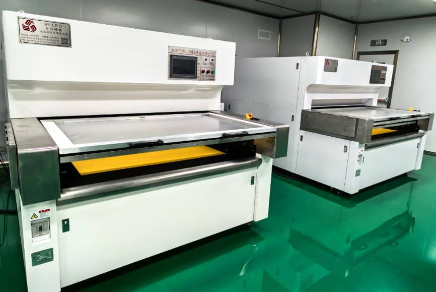
Imaging
Circuit patterns are exposed onto each inner layer.
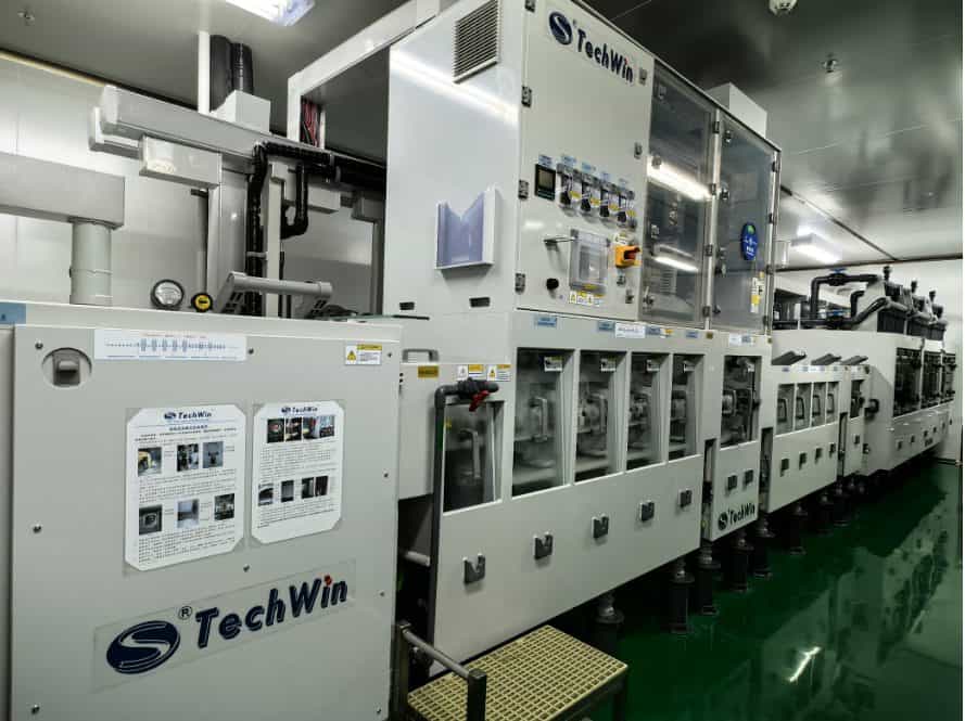
Developing and etching
Layers are developed and etched, then checked by automated optical inspection before lamination.
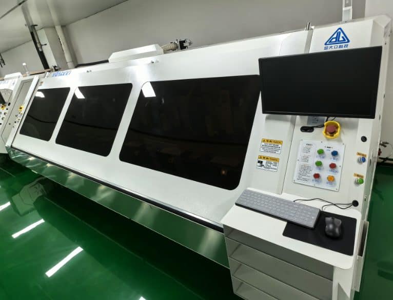
Lamination, drilling and plating
Layers are pressed, drilled mechanically or by laser, and hole walls are plated. Vias are plugged or filled where specified.
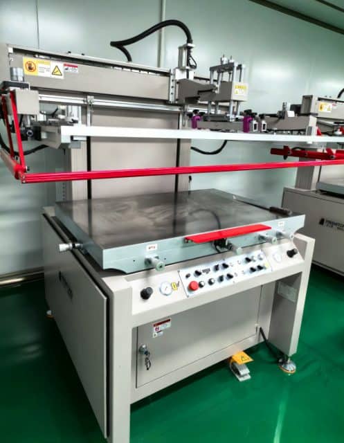
Solder mask and finish
Solder mask is printed and cured; ENIG thickness is measured by XRF on every lot.
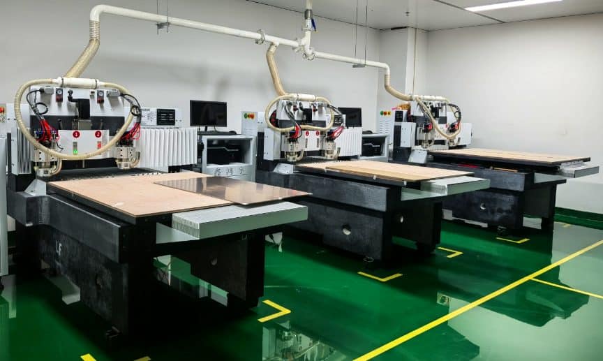
Profiling
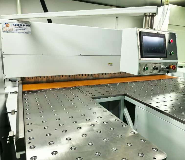
Boards are routed or V-scored to your outline and panel drawing.
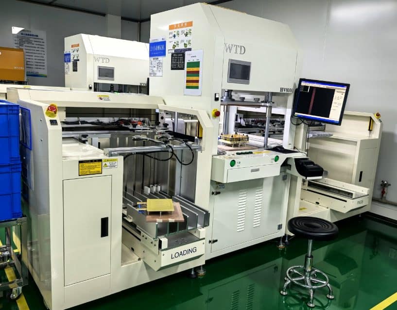
Electrical test and inspection
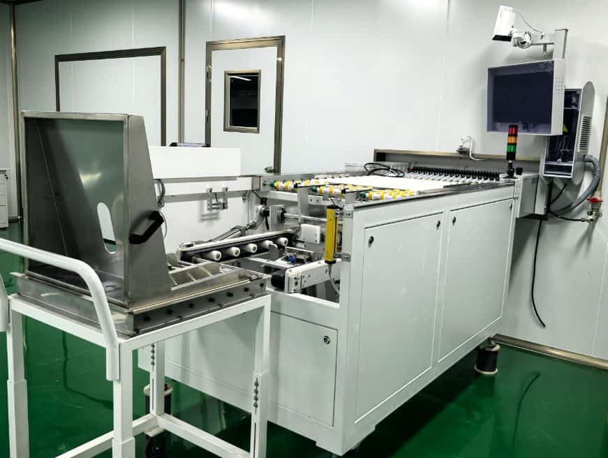
Every bare board is 100% electrically tested, then inspected to the IPC class on your order. See a sample QC report.
Weighing layer count? Read 4-layer vs 6-layer PCB and 6-layer vs 8-layer PCB.
Landed cost
What Adds to the Price of a PCB Ordered from China
The board price on a quote is only part of what you pay. Our boards are manufactured and shipped from China, so the country of origin on your customs paperwork is China.
- Board priceDriven by layer count, material, board area, finish and quantity.
- Import dutyDepends on how the board is classified. Our HS code guide for PCB and PCBA explains it.
- Freight and lead timeAir freight cost against how long you can wait.
- Rework riskWhat a failed lot costs in re-spins and schedule.
Quality
Quality System and Build Classes
In-house checks include 100% electrical test on bare boards, XRF measurement of ENIG on every lot, and bare-board solderability testing.
| Class 2 | Class 3 | |
|---|---|---|
| Typical products | Industrial, telecom, consumer electronics | Medical, aerospace and other high-reliability products |
| What changes | Standard plating and annular ring limits | Tighter plating, annular ring and void limits; hole wall copper ≥25 µm |
More detail: IPC Class 2 vs Class 3 PCB.
Industries & projects
Boards for Demanding Products
CGM HDI PCB case study
A wearable glucose monitor board reduced from 12 layers to 8 with stacked microvias.
5G small cell PCB case study
Rogers 4350B boards held to ±3.5% impedance across 2,000 units.
IGBT ceramic PCB design review
What to check before releasing a ceramic power substrate to production.
Ordering
Quotes, Lead Times and Quantities
Bare-board quotes within 2 hours of receiving complete files, Mon–Sat 9AM–6PM CST.
No minimum order. Prototypes start from 1 piece.
2–4 layer FR-4 prototypes are free for new customers.
Reference lead times by layer count and board area are on our home page; your quote confirms the ship date. Expedited builds available.
We build to the panel drawing you supply.
Gerber or ODB++, drill files, and fabrication notes covering material, thickness, copper, finish and IPC class.
Tools & guides
PCB Engineering Tools and Guides
FAQ
PCB Manufacturing FAQ
What is the difference between PCB fabrication and PCB assembly?
Fabrication makes the bare board; assembly mounts the components. We do both. See SMT assembly for assembly.
How many layers can you build?
Standard builds go up to 24 layers. Advanced builds with engineering review go up to 100 layers. See multilayer PCB.
Can you build to IPC Class 3?
Yes. Boards are built and inspected to IPC-6012 / IPC-A-600 Class 2 or Class 3, as specified on your order. See Class 2 vs Class 3.
Is there a minimum order quantity?
No. Prototypes start from 1 piece, and 2–4 layer FR-4 prototypes are free for new customers.
How fast can I get a quote?
Bare-board quotes are returned within 2 hours of receiving complete files during business hours.
What lead time should I plan for?
It depends on layer count and board area. Reference lead times are on our home page, and your quote confirms the ship date.
Do you offer via-in-pad?
Yes: filled and capped vias (IPC-4761 Type VII), plus resin plugging. See via tenting vs plugging vs filling.
Which surface finish should I choose?
We offer ENIG, ENEPIG, OSP and HASL. The right one depends on pad pitch, shelf life and assembly method; our ENIG guide explains when ENIG fits.
What files do I need to send?
Gerber or ODB++ files, drill files, and fabrication notes covering material, thickness, copper weight, finish and IPC class.
Get a PCB Quote in 2 Hours
Send your Gerber files and fabrication notes. A CAM engineer reviews them and returns a bare-board quote within 2 hours during business hours.