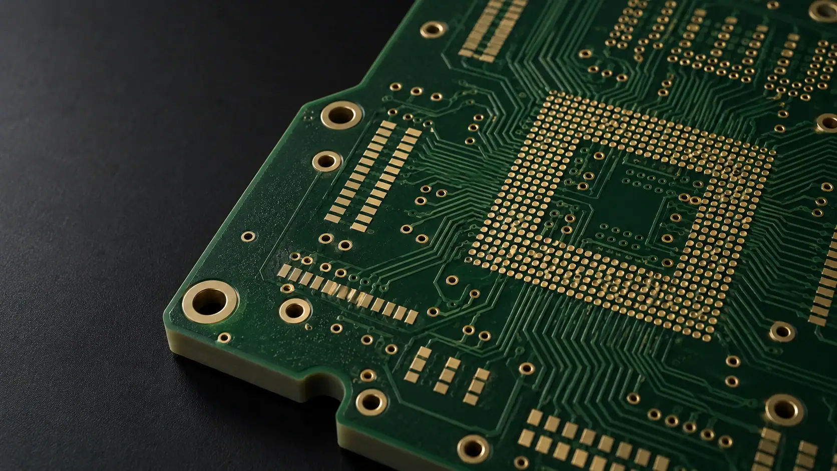
Close-up of a dense multilayer semiconductor test interface PCB with fine routing and an array of plated contact pads
Load board · probe card · burn-in board PCBs

ATE PCB Manufacturing for Semiconductor Testing

An interface mismatch found at bring-up can mean another board build. Confirm the outline, stackup and acceptance requirements before fabrication. QueenEMS builds load board, probe-card and burn-in PCBs to your released design data.

  • Interface drawing reviewed before fabrication
  • Stackup, impedance and finish agreed before release
  • Repeat builds tied to one approved revision
Send Files for Review

Request an ATE PCB Review

An email is enough to start. Add a short project note or files if you have them.

One file up to 50 MB: ZIP, RAR or Gerber/drill layers. Put PDF drawings, ODB++ and multiple files in one ZIP or RAR archive.

Only email is required.

Illustrative image.

Three things to close before an ATE PCB order is released

  • FitOutline, holes, thickness, flatness and contact finish
  • ConstructionStackup, laminate, impedance and via structure
  • RevisionWhat may and may not change between builds
Procurement risks

Resolve These ATE PCB Risks Before Release

Each risk below is a common gap between design intent and the board that gets built. Each one maps to a specific review input and a written acceptance point.

RISK 01

Fit or flatness mismatch found after fabrication

What it costsMounting holes, the stiffener interface, flatness or contact-pad finish can differ from the test hardware requirements. A mismatch found at bring-up can delay the project and require a revised board build.
Agreed before releaseSend the interface drawing, thickness tolerance and flatness limit with the area it applies to. Agree the dimensional checks, flatness measurement method and contact-area finish during quotation.
RISK 02

Stackup, material and impedance left open

What it costsUnspecified laminate, dielectric thickness, impedance targets or finish leave room for different interpretations. The fabricated construction can then differ from the design assumptions.
Agreed before releaseSubmit the proposed stackup and impedance table for feasibility review. Confirm any proposed trace, dielectric or laminate changes before approval, and reference the agreed stackup, coupon requirements and finish on the order.
RISK 03

Prototype and repeat builds drift apart

What it costsTest hardware is often reordered months or years later. Without a frozen revision, a laminate, finish or drill change can enter the repeat build unnoticed.
Agreed before releaseReference one approved drawing and data revision on each order. Agree how any laminate, finish, stackup or drill changes will be reviewed and approved before a repeat build.

Send the drawing package you have and identify the questions to resolve before fabrication.

Start an Engineering Review
Board families

Load Board, Probe Card and Burn-in Board PCBs

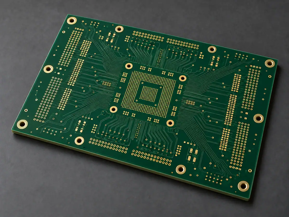
Bare load board PCB with a central device-under-test footprint, mounting holes and dense routed layers
Final test

Load Board PCB

Connects packaged devices to the tester through sockets, relays and signal-conditioning parts.

  • Tester interface outline, mounting and stiffener holes
  • Site count and socket footprint per DUT
  • Impedance-controlled nets and per-site power paths
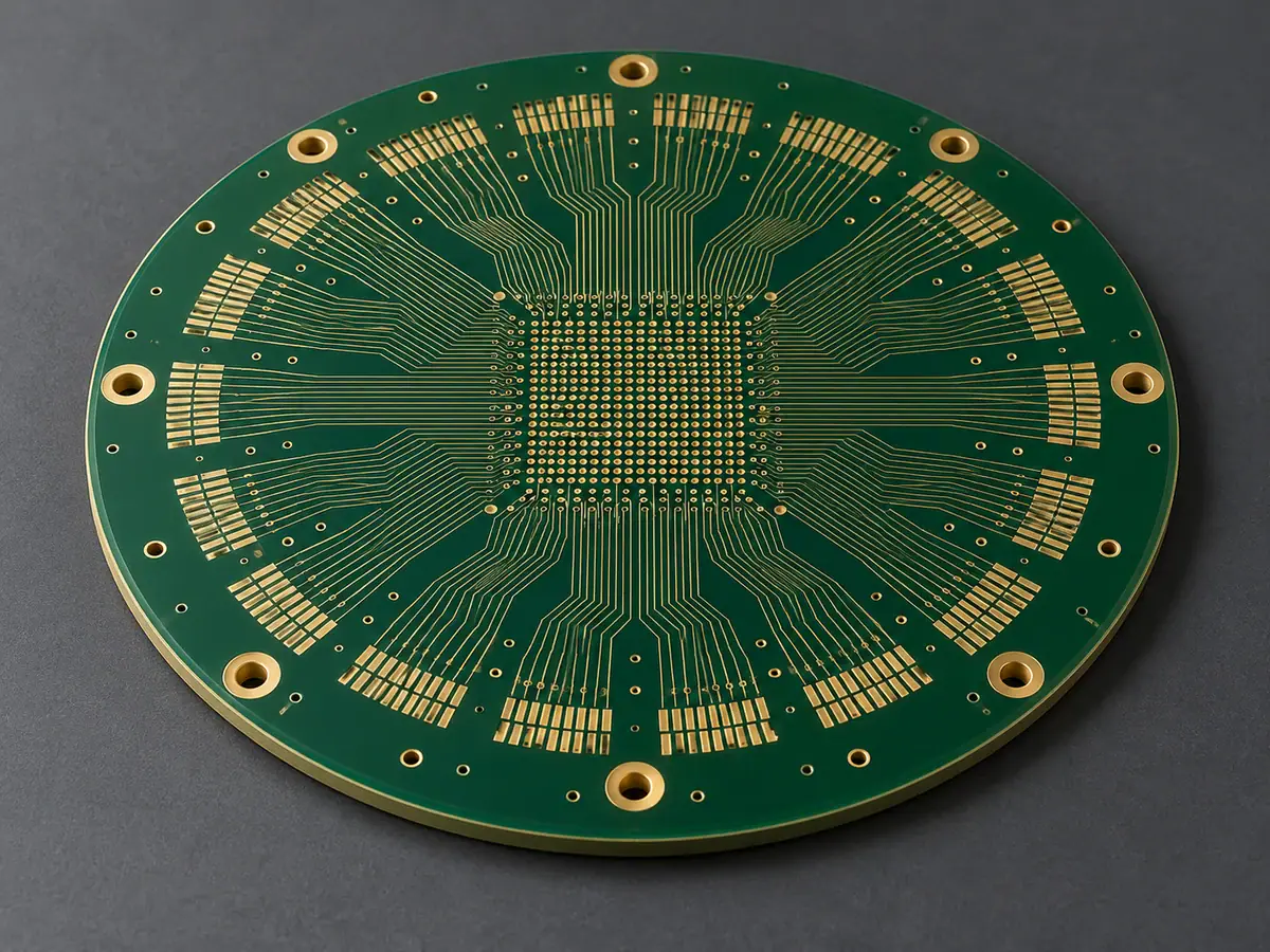
Bare round probe card PCB with a central contact-pad array and radial signal routing
Wafer sort

Probe Card PCB

Carries signals between the tester interface and the probe head while wafers are probed.

  • Outline and mounting features for your prober and probe head
  • Pad array for the probe-head interface
  • Planarity requirement over the interface area
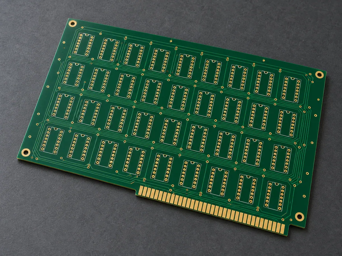
Bare burn-in board PCB with repeated socket footprints in a grid and a card-edge connector
Reliability stress

Burn-in Board PCB

Holds many devices in sockets under bias and elevated temperature inside a burn-in chamber.

  • Chamber slot dimensions and edge-connector layout
  • Operating temperature and exposure duration
  • Current per site and required copper weight

Illustrative PCB configurations; final construction follows the approved design.

Application fit

Which Test Board Are You Buying?

The board family decides which drawing matters first. Each review starts with the document that defines the interface the board must meet.

Scroll sideways to see all columns.

Board familyWhere it worksInterface it must matchFirst document we reviewWhat we build
Load board PCBFinal test of packaged devicesTester interface outline, socket footprints, stiffener mountingMechanical interface drawing with holes and keep-outsBare PCB to your approved data; assembly to an agreed BOM when quoted
Probe card PCBWafer sortProber mounting and the probe-head pad arrayOutline and pad-array drawing with the planarity area markedThe printed circuit board; probe head and card assembly stay with your supplier
Burn-in board PCBDevices under bias and temperature in a chamberChamber slot, edge connector and socket gridSlot and edge-connector drawing with operating temperatureBare PCB in the laminate you specify or approve; socket fitting only when quoted
Other DUT or interface boardHandler, bench or fixture interfacesYour mechanical and connector definitionFabrication drawing and stackupBare PCB to your approved data
Construction decisions

Close the Stackup Before the Price Is Final

Layer construction and material availability affect price and feasibility. Confirm these details during review so the quotation matches the approved build.

  1. Layer count and orderSignal, plane and power layers in sequence, as you designed them.
  2. Dielectric systemThe laminate family you designed with, or the properties it must meet.
  3. Thickness per layer and finished thicknessIncluding the tolerance that applies at the interface area.
  4. Copper weight per layerSignal layers and current-carrying planes stated separately.
  5. Via structureThrough, blind, filled or back-drilled vias, and where each is used.
  6. Surface finish by regionOne finish or different finishes for contact areas and the rest of the board.
Signal and power

Electrical Requirements, Written Into Acceptance

You define the electrical intent in your design data. We confirm what the fabricated board will be built and checked against.

Signal paths

You supply

  • Impedance targets per net class, with reference layers
  • Single-ended and differential trace definitions
  • Length-matched groups as routed in your layout

Agreed on the order

  • Trace or dielectric adjustments, approved before release
  • Impedance coupons and measurement method, where required

Power delivery

You supply

  • Current per site or per rail
  • Copper weight per layer and plane allocation
  • Heavy-copper regions and their location in the stackup

Agreed on the order

  • Copper weights stated on the fabrication drawing
  • Bare-board electrical test coverage, such as flying probe

Agree which board-level checks verify the released fabrication requirements. Your test engineering team validates channel performance on the tester.

Mechanical and contact areas

Where Test Hardware Meets the Board

An unmarked hole tolerance or contact keep-out can become a fit problem after fabrication. Put these requirements on the drawing before release.

Interface geometry

  • Outline and datum scheme
  • Mounting, alignment and stiffener holes with tolerances
  • Component and probe keep-out zones
  • Thickness at the interface region

Contact surfaces

  • Finish for each contact region: socket, pogo pin or probe-head pads
  • Solder mask clearance around contact pads
  • Areas that must stay free of silkscreen or marking

State the area, not just the number

A flatness limit means little without the region it applies to and how it is measured. Mark the area on the drawing and agree the measurement method during quotation.

Socket and stiffener supply or fitting is quoted case by case when you need it.

Acceptance & evidence

What Is Written Down Before the Board Is Built

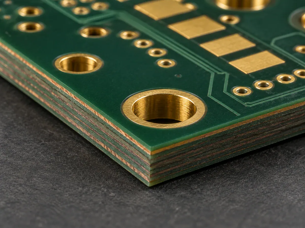
Macro view of a multilayer PCB edge and plated holes, illustrating stackup and via review
Illustrative image; final construction follows the approved design.
Fabrication scope We build the PCB to your released data and the acceptance agreed on the order, and assemble to an agreed BOM only when that is quoted. Interface design, probe-head supply, test programs, calibration and device correlation stay with your engineering team. Any socket or mechanical integration is scoped separately during quotation.

Your input, and the acceptance it becomes

Use these points to agree what will be checked and recorded for your project.

AreaYour inputAcceptance on the order
StackupLayers, dielectrics, copper weights, finished thicknessApproved stackup drawing revision
ImpedanceTargets per net class and reference layersCoupon and measurement method, if required
MechanicalOutline, holes, stiffener interface, tolerancesDimensional check method and sampling
FlatnessLimit and the area it applies toMeasurement method agreed in writing
Contact finishFinish for socket, pogo-pin or probe areasFinish callout on the fabrication drawing
WorkmanshipIPC class and electrical test expectationsClass and test coverage stated on the order
Inspection, matched to the agreed scope AOI, X-ray and flying probe test are available for fabrication; ICT and functional testing apply to assembled boards under an agreed procedure. Methods and coverage are set per project, not applied to every board by default.
  • Approved stackup revision
  • IPC class on the order
  • Electrical test coverage
  • Material declarations you require
RFQ package

Start With What You Have, Add the Rest by Release

Only your email is required to inquire. Add the information you have so we can identify the next review step.

  1. To start a review

    • Business email
    • A short note, if available: board family, layer count, quantities
    • Any files you already have
  2. To quote

    • Gerber or ODB++ with drill data
    • Stackup and impedance table
    • Fabrication drawing with finish and flatness requirements
    • IPC class and quantities for prototype and repeat
  3. Before release

    • Final data revision and approved stackup
    • Agreed checks and records for the order
    • BOM and placement file if assembly is quoted

Uploading files

Use the inquiry form at the top of this page. Upload one ZIP, RAR or Gerber/drill file up to 50 MB; put PDF drawings and ODB++ data inside a ZIP or RAR archive.

Assembly and timing

Assembly is optional, with turnkey parts through Mouser, DigiKey or LCSC, or your consigned material. PCB lead time is quoted per material and construction. Our PCBA work typically takes about 5–8 working days once all materials are ready.

How a project runs

From Design Files to Shipped Boards

  1. Send files

    Gerber or ODB++, drill data, drawing, stackup and interface constraints.

  2. Feasibility review

    Specific questions and proposed adjustments come back to you.

  3. Agree acceptance

    Agree stackup, finish, IPC class, checks and change approval in writing.

  4. Build and inspect

    Fabrication, plus assembly if quoted, checked by the agreed methods.

  5. Ship with records

    Boards ship with the records agreed in step 3.

Lead time depends on material availability and construction and is confirmed with the quotation. For a general manufacturability check on draft data, see our PCB DFM review.

Prototype to repeat

Build It Again the Way You Approved It

Test hardware is often reordered long after the first build. Fix the reference points while the prototype is fresh.

Record at first approval

Release version
Drawing and data revision the build was made from
Construction
Approved stackup, laminate and finish
Acceptance
IPC class, test coverage and checks agreed for the order
Records
The inspection records agreed for that order

Treat as a change

  • Laminate
  • Surface finish
  • Stackup or layer thickness
  • Copper weight
  • Drill program
  • Outline or holes

Agree who reviews and approves each change before a repeat build, and reference the approved revision on every order. Prototype acceptance and production acceptance can be defined separately when early builds are engineering samples.

Why QueenEMS

Working With QueenEMS

More than 10 years

QueenEMS and Queenpcb Limited are the same company, supporting PCB fabrication and assembly projects for over a decade.

Your IPC class

Requirements are reviewed against the class on your order, including IPC Class 3 when the project calls for it.

Fabrication and PCBA

Turnkey parts through Mouser, DigiKey or LCSC, or your consigned material, assembled to an agreed BOM and process.

Scope stated up front

You know which requirements we confirm and which stay with your test engineering team before an order is placed.

FAQ

ATE PCB Purchasing Questions

Do you design load boards or probe cards?

No. We fabricate PCBs from your design data and review them for manufacturability. Interface design, test programs and calibration stay with your team or your design partner.

Can you supply an assembled load board with sockets installed?

We can assemble components to an agreed BOM and process. Socket supply, socket installation, stiffeners and tester integration are confirmed case by case during quotation; they are not included by default.

Can you meet my impedance, flatness and layer-count requirements?

We confirm this per design at feasibility review. Send the stackup, impedance table and flatness limit with the area it applies to. Our conventional multilayer range runs up to 24 layers; higher-layer constructions are assessed individually.

What do you need for a quotation?

Gerber or ODB++ with drill files, a fabrication drawing, the stackup, impedance targets, the required IPC class and quantities. Add the BOM and placement file if assembly is in scope. Partial data is fine for a first review.

How long does an ATE PCB take?

Fabrication lead time depends on material availability and construction, so it is quoted per project. As a general guide for our PCBA work, assembly takes about 5–8 working days once all materials are ready; ATE build schedules are confirmed with each order.

Can we start with a prototype and move to repeat builds?

Yes. Record the approved stackup, materials and acceptance requirements at the first build, then reference the same revision on repeat orders. Any change to laminate, finish, stackup or drill data should be approved before it is built.

Close the Open Questions Before You Release the Board

Send an email address and whatever data you have. We come back with feasibility questions and a quotation for the agreed construction.

  • Design data: Gerber or ODB++, drill files and fabrication drawing
  • Construction: stackup, impedance targets and flatness limit
  • Acceptance: IPC class, test coverage and records you need

Send Your Project for Review

An email is enough to start. Add a short project note or files if you have them.

One file up to 50 MB: ZIP, RAR or Gerber/drill layers. Put PDF drawings, ODB++ and multiple files in one ZIP or RAR archive.

Only email is required.