
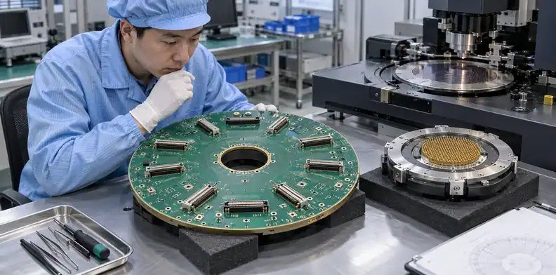
Quick Answer: Probe card manufacturing combines a custom PCB or interface board with a probe head, contact elements, mechanical hardware, and calibration work. A PCB fabricator can build the routed board, but it does not automatically supply the complete wafer-probing assembly. Before requesting a PCB quote, define the tester interface, probe-head boundary, signal classes, stackup, materials, routing constraints, via structures, planarity controls, inspection evidence, and final electrical tests. Keep the wafer-contact technology and probe-head integration with the qualified owner unless the quotation explicitly includes them.
A probe card sits between automated test equipment and the devices on a semiconductor wafer. The board fans tester resources out toward the probe head while carrying power, ground, digital, analog, and sometimes RF paths. A small layout or stackup change can therefore affect signal loss, contact stability, mechanical alignment, or the ability to calibrate the final assembly.
This guide is for test engineering, hardware, sourcing, and quality teams preparing a probe card PCB request. It explains the PCB manufacturing package and its release evidence. It does not treat a bare PCB factory as a substitute for a probe-card designer, MEMS probe supplier, or wafer-test integrator.
Table of Contents
- What Is a Probe Card PCB?
- Where Does the PCB Manufacturing Scope End?
- Which Electrical Requirements Drive the Stackup?
- How Should Materials and CTE Be Specified?
- How Should Dense I/O Routing Be Planned?
- Which Via and Pad Structures Need Early Review?
- What Fabrication Controls Protect Alignment and Planarity?
- How Should the PCB Be Tested and Released?
- What Belongs in the Probe Card PCB RFQ?
- How Do You Qualify a Probe Card PCB Supplier? – FAQ
What Is a Probe Card PCB?
A probe card PCB is the routed electrical interface inside a wafer-test probe card. It connects the automated test equipment, usually through a tester-side interface, to a probe head that places physical contacts on wafer pads, bumps, or pillars. The exact construction varies, but the PCB commonly distributes power and ground, maps tester channels, supports conditioning components, and provides the mechanical reference used by the surrounding assembly.
The finished probe card is custom to the device, tester, prober, contact technology, and test conditions. A change in pad map or die shrink can require a different contact layout and channel map. The PCB is one part of that system. Other parts may include cantilever needles, vertical probes, MEMS contacts, ceramic or organic space transformers, stiffeners, support plates, connectors, housings, and calibration structures.
The practical purchasing term is often “probe card,” but the requested item may be only a bare probe card PCB, a populated interface board, a probe-head subassembly, or a complete calibrated card. Put the item name and ownership boundary on the quotation. Otherwise, one supplier may price a bare board while another prices an integrated test interface, making cost and lead-time comparisons meaningless.
Probe card and DUT-board terminology also overlaps across test organizations. Some teams use DUT board for package-level testing and probe card for wafer-level contact. Others use interface-board names more broadly. Use controlled drawings and interface definitions instead of relying on the label alone.
Where Does the PCB Manufacturing Scope End?
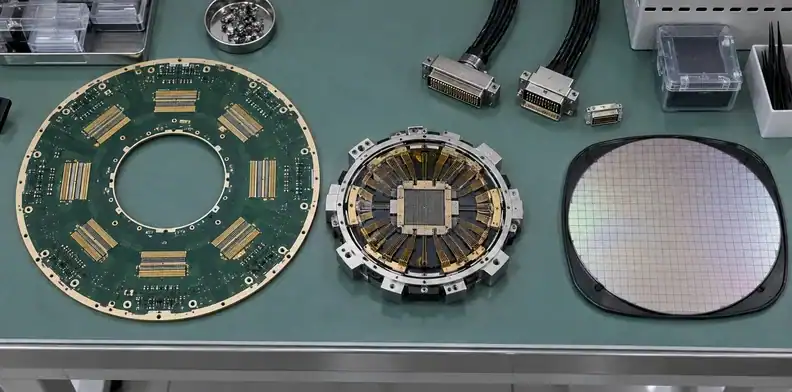
The PCB manufacturing scope usually covers laminate procurement, multilayer fabrication, drilling, plating, imaging, lamination, surface finish, routing, electrical test, inspection, and the agreed documentation package. Assembly scope may add connectors, passive components, relays, sockets, shields, or other board-level hardware. The probe head, contact elements, precision alignment, contact-force setup, scrub behavior, calibration, and wafer-level correlation normally require specialist ownership.
Do not infer full-system capability from the phrase “probe card manufacturing.” Ask each supplier to mark the boundary in writing. A board that passes bare-board continuity can still fail after probe-head integration if the layout, stackup, contact transition, or mechanical datum was wrong. The PCB fabricator needs approved interface data from the probe-card designer, and the integrator needs fabrication evidence from the board supplier.
| Deliverable | Typical PCB fabricator responsibility | Responsibility that needs explicit confirmation |
|---|---|---|
| Bare multilayer board | Materials, stackup, copper, vias, finish, outline, electrical test | Final probe-card calibration and wafer correlation |
| Component assembly | Approved BOM, placement, soldering, cleaning, inspection | Tester software, probe setup, and device test program |
| Mechanical features | Routed outline, holes, slots, thickness, agreed tolerances | Probe-head alignment, overtravel, force, and scrub setup |
| Contact interface | Pads, routing, plating, connector footprints | Needles, vertical contacts, MEMS structures, or space transformer |
| Release evidence | COC, material records, dimensions, test reports, inspection data | System-level contact resistance, leakage, RF calibration, and wafer results |
Write exclusions beside inclusions. If the quote covers the PCB and connector assembly but excludes the probe head, state who supplies the probe head, who performs final integration, and which party owns failures at the transition. That short scope note prevents the most expensive type of procurement error: receiving a technically correct component that cannot be released as a working probe card.

Which Electrical Requirements Drive the Stackup?
The stackup should start from the signal classes and test limits, not a preferred layer count. Separate power delivery, sensitive analog measurements, high-speed digital paths, clocks, RF channels, guards, sense lines, and grounds. For each class, provide the electrical requirement that the PCB can control and verify. The fabricator cannot convert a tester bandwidth or device test limit into a stackup without the routing topology and interface design.
Map the Current Return Path
Every controlled path needs a defined return. Specify reference planes, layer transitions, stitching strategy, connector return pins, and any split-plane restrictions. A trace may meet its nominal impedance in a coupon while the assembled channel performs poorly because a reference-plane change or connector breakout interrupts the return path.
Power distribution also belongs in the stackup review. Give current, voltage, allowed drop, transient behavior, and sense topology for each relevant rail. High-current paths may need wider copper, heavier copper, parallel layers, multiple vias, or remote-sense routing. Keep force and sense paths distinct where the measurement architecture requires it.
Define What “Controlled” Means
Controlled impedance requires the target, tolerance, trace geometry, copper weight, dielectric information, reference layer, and test method. The controlled impedance PCB requirements guide explains the fabrication inputs. For mixed laminate or unusual routing, the high-frequency hybrid stackup RFQ guide covers the evidence needed before a hybrid construction is released.
| Signal class | PCB inputs to define | Release evidence to request |
|---|---|---|
| DC power and ground | Current, drop limit, copper path, via current, sense points | Netlist test, copper/stackup record, relevant resistance check |
| Precision analog | Guarding, leakage target, spacing, contamination controls | Cleanliness evidence, leakage or insulation test when specified |
| High-speed digital | Single-ended or differential target, reference planes, skew constraints | Coupon report, stackup as-built, channel review where contracted |
| RF | Frequency range, impedance, launch, loss budget, calibration boundary | Material lot data, impedance evidence, RF test plan if included |
| Clocks and triggers | Edge rate, timing relationship, fanout, return path | Routing review and agreed timing evidence |
Do not ask the fabricator to “keep signals clean” without measurable limits. Give the owner, target, tolerance, and verification method for each controlled feature. If the test system team will perform system-level calibration later, the RFQ should still identify which board properties must be proven before integration.
How Should Materials and CTE Be Specified?
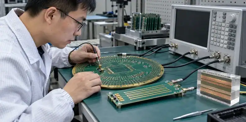
Material selection affects electrical loss, dimensional movement, thickness stability, drilling, plating, assembly temperature, and long-term mechanical behavior. A generic “high Tg” callout does not define Dk, Df, z-axis expansion, moisture behavior, resin content, copper treatment, or the test frequency behind the datasheet value.
Start with the functional need. If the board carries high-frequency or low-level measurement paths, state the relevant frequency range and loss or phase concern. If the assembly uses tight mechanical alignment, identify the temperature range and which dimensions must remain controlled. If the board sees repeated thermal cycling or heavy connector hardware, include the reliability conditions that matter to plated holes and the mechanical stack.
Control Substitutions Before Tooling
List the approved material by manufacturer and grade where qualification depends on it. If alternatives are allowed, define the properties and evidence that must match. The PCB material substitution approval guide provides a controlled route for reviewing a proposed replacement instead of accepting a same-Tg claim.
Probe card work may also sit near IC-substrate terminology. A fine-feature BT substrate and a conventional multilayer PCB are not interchangeable simply because both route dense signals. The BT substrate vs HDI PCB guide separates those build routes. Use it when the design includes substrate-like pitch, laser vias, or packaging constraints that may exceed a normal PCB process.
| Material concern | What the drawing or RFQ should state | Supplier evidence |
|---|---|---|
| Electrical behavior | Dk/Df basis, frequency, loss concern, impedance targets | Datasheet revision, lot identity, impedance or loss evidence as agreed |
| Thermal movement | Operating/assembly range, CTE-sensitive dimensions | Material CTE data and dimensional inspection plan |
| Thickness and flatness | Finished thickness, local limits, bow/twist or flatness definition | Measured map, method, fixture, and sampling plan |
| Plated-hole reliability | Copper weight, hole structure, thermal exposure | Coupon or section evidence when specified |
| Material substitution | Approved grades or property-based approval route | Written deviation with comparative data before use |
State whether material certificates, lot traceability, microsections, or coupons are required with prototypes and production lots. Evidence that arrives only after a dimensional or electrical failure is late. Put it in the quotation package so the supplier can price the inspection and retain the right samples.
How Should Dense I/O Routing Be Planned?
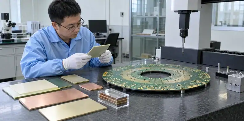
Dense I/O routing begins with the channel map, connector architecture, probe-head transition, and keepout geometry. Freeze those interfaces before asking for final DFM. A routing team cannot protect skew, crosstalk, leakage, or current capacity if nets arrive as anonymous labels with no electrical class.
Group Nets by Behavior
Give each net class its required width/spacing rule, reference layer, via policy, length or skew constraint, shielding need, and test priority. Separate sensitive measurement nodes from clocks and fast digital lines. Keep high-current paths away from low-level sense nodes where coupling or temperature rise could alter the measurement. Define guard structures only with the test engineer who owns the leakage path; a guard tied to the wrong potential can make the measurement worse.
Breakout density may force blind vias, buried vias, stacked or staggered microvias, via-in-pad, sequential lamination, or smaller mechanical holes. Each added structure changes cost, yield, inspection, and repair options. Do not approve the layer count before the escape pattern and via architecture have been reviewed together.
Preserve Calibration and Debug Access
Reserve the pads, connectors, coupons, fiducials, and test access needed by the integration team. A board that routes every channel but removes access to calibration or fault isolation can lengthen probe-card bring-up. Mark do-not-probe areas as well as intended test points so a factory fixture does not load a sensitive node.
Use the PCB source netlist and the probe-card channel map as separate controlled records. The netlist proves PCB connectivity. The channel map proves that the correct tester resource reaches the intended probe-head contact. Comparing both catches a class of mapping errors that a standard bare-board electrical test cannot detect.

Which Via and Pad Structures Need Early Review?
Review via types before layout density locks the build into a process that only a narrow supplier set can manufacture. For each structure, define finished diameter, pad size, aspect ratio, copper requirement, fill or cap condition, sequential-lamination cycle, and the reason it is needed. The final numbers should come from the selected fabricator’s qualified capability and the design authority’s reliability limits.
Via-in-pad may be useful under dense connectors, BGAs, or transition structures, but an open or poorly filled via can pull solder, disturb coplanarity, or leave an uneven pad. Specify whether the via is resin filled, copper filled, capped, planarized, and plated over. Identify which pads carry assembly, contact, or measurement functions because the same visual defect can have different consequences at each location.
Laser microvias require extra attention at stacked interfaces. Copper thickness, capture-pad alignment, dielectric thickness, registration, and thermal history affect the joint. The PCB laser drilling guide explains the fabrication controls that belong in an HDI review. Do not turn a microvia type into a purchasing shorthand without the stackup and section detail that define it.
Large press-fit or connector holes create a different risk. Their finished size, plating, tolerance, breakout, and annular ring must match the hardware and insertion process. Ask the assembly owner for connector drawings and tolerance assumptions before the board drawing is released. A hole that passes the bare-board gauge can still damage a compliant pin if the combined tolerance stack was wrong.
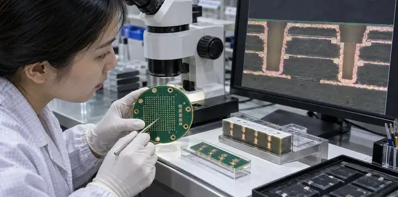
Include dedicated coupons when the release plan needs plated-hole or microvia section evidence. The coupon must represent the relevant stack and process. A generic panel coupon does not automatically represent every via structure on a complex board.
What Fabrication Controls Protect Alignment and Planarity?
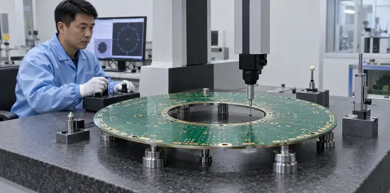
Probe-card integration depends on the relationship among holes, fiducials, connector features, board outline, local pads, and the probe-head datum. Put that relationship on a controlled drawing. A general outline tolerance does not protect a critical hole-to-fiducial position unless the datum scheme and measurement method make the requirement clear.
Panelization and copper balance can affect movement through lamination and assembly. Ask the supplier how the critical dimensions are compensated and inspected, but do not prescribe undocumented scaling factors from a previous factory. The fabricator owns its process compensation; the buyer owns the finished requirement and the evidence needed to accept it.
Planarity also needs a functional definition. Name the area, support condition, temperature, measurement grid, and maximum permitted deviation. Whole-board bow and twist may not describe a local interface surface under a stiffener or probe head. If assembly hardware changes the shape, define whether inspection occurs on the free board, after component assembly, after stiffener installation, or at several stages.
Surface finish and pad flatness should match the assembly and contact process. Specify which areas receive which finish, whether selective finishes are allowed, and how thickness or coverage is verified. Keep solder mask, legend, adhesive, and repair material away from precision mating or grounding regions unless the design intentionally uses them.
Before the purchase order, run a joint design review covering stackup, materials, controlled dimensions, via structures, finish, panelization, tooling, coupons, and release documents. The PCB DFM review before PO guide gives sourcing and engineering a shared closure list.
How Should the PCB Be Tested and Released?
Release testing should separate bare-board proof from assembled-interface proof. A bare-board netlist test checks opens and shorts against the PCB data. It does not prove channel mapping to the tester, contact behavior at the wafer, RF calibration, leakage in the final environment, or the mechanical setup of the probe head.
Match Each Risk to Evidence
Request the evidence that closes the controlled risk. Impedance coupons support transmission-line verification. Microsections support plated-hole or microvia review. Dimensional reports support alignment and thickness. Insulation or leakage tests may support sensitive nodes when the acceptance method is defined. Material records support the stackup and substitution decision.
For controlled impedance, specify coupon design, test method, frequency basis where relevant, limits, and reporting. The PCB impedance test report guide shows what a useful report identifies. For connectivity and isolation, use the PCB electrical test requirements guide to define netlist, test voltage or thresholds where applicable, and traceable pass records.
| Release layer | Question answered | Evidence owner |
|---|---|---|
| Material and stackup | Was the approved construction used? | PCB fabricator |
| Connectivity and isolation | Does the board match the approved netlist? | PCB fabricator |
| Controlled electrical features | Do agreed impedance, leakage, or resistance checks pass? | Fabricator or named test laboratory |
| Mechanical interface | Are datums, holes, thickness, and local planarity within limits? | Fabricator and integration owner |
| Channel mapping | Does each tester resource reach the intended transition/contact? | Probe-card designer or integrator |
| System calibration and wafer correlation | Does the complete assembly measure the device correctly? | Test engineering and probe-card integrator |
Archive as-built stackup, material lot, deviation approvals, dimensional data, electrical reports, microsection images when required, and the final channel map under the same revision identity. A pass label without the revision and test basis cannot support a future repeat order or failure review.

What Belongs in the Probe Card PCB RFQ?
An RFQ should let the supplier identify the build route, inspection cost, capability gaps, and interface risks before quoting. Send controlled fabrication data, not screenshots or a previous board alone. Include Gerber or ODB++, drill and rout data, IPC-356 or another approved netlist where available, stackup, fabrication drawing, material requirements, impedance data, component data for assembly, and the mechanical interface drawing.
The probe-card-specific package should add the tester and prober interface, probe-head boundary, channel-map owner, critical datums, local planarity area, restricted repair areas, cleanliness controls, calibration features, and the release evidence list. Mark which data is final and which remains for engineering review.
| RFQ item | Minimum useful content | Question it closes |
|---|---|---|
| Product scope | Bare PCB, assembled PCB, mechanical hardware, probe head, integration exclusions | What is the supplier actually quoting? |
| Fabrication package | PCB data, netlist, drawing, stackup, materials, finish | What must be built and inspected? |
| Electrical intent | Net classes, impedance, current, leakage, skew, RF range | Which features need controlled routing or test? |
| Mechanical interface | Datums, holes, outline, thickness, local planarity, stiffener state | What must align during integration? |
| Via and pad definitions | Via types, fill/cap, pads, sequential lamination, coupons | Which qualified process route is required? |
| Evidence package | Reports, certificates, sections, dimensions, traceability, deviation flow | What proves the lot is releasable? |
| Commercial inputs | Prototype quantity, production estimate, target date, delivery location | What pricing and lead-time basis should be used? |
Ask suppliers to return questions and exceptions in writing. A proposed material, via, finish, stackup, test, or tolerance change should not disappear inside the quotation. Record the approved answer and update the controlled file when the design changes.
If the files are not ready for quotation, use a free PCB DFM check to identify fabrication questions first. Keep the review at the PCB boundary unless a named partner owns the complete probe-card integration.
How Do You Qualify a Probe Card PCB Supplier?
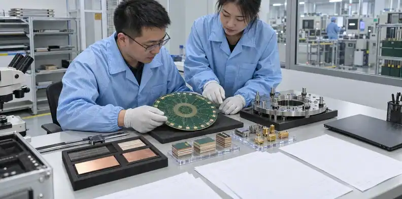
Qualify the process route, evidence system, and communication discipline, not a broad claim that the supplier makes advanced boards. Start with a representative prototype that includes the real stackup, smallest vias, controlled features, critical dimensions, local planarity requirement, and intended surface finish. A simplified coupon board may prove one process, but it does not prove the complete interface.
Review the supplier’s response to risk. A qualified supplier should identify ambiguous data, distinguish PCB tests from system tests, propose measurable alternatives, and refuse limits it cannot verify. Ask who reviews CAM, impedance, materials, microvias, dimensional control, assembly, and final records. The quality of those answers often predicts the quality of the build record.
Use first-article evidence to close the agreed risks. Compare as-built stackup and material records with the approved package. Review cross-sections and impedance data where required. Check critical dimensions and the stated support condition for planarity. Confirm that deviations were approved before manufacture, not documented after the parts were complete.
Then run integration evidence under the probe-card owner: mechanical fit, channel mapping, contact continuity, leakage, RF or timing calibration where applicable, thermal behavior, and wafer correlation. Feed any PCB-related finding back into the drawing or acceptance plan before the repeat order.
A production release should name the approved factory and process route, frozen data revision, allowed materials, required reports, change-notification rules, and requalification triggers. To review a real design package, contact QueenEMS with the PCB files, stackup, interface drawing, and required evidence. State clearly whether you need a bare board, component assembly, or support coordinating with a separate probe-card integrator.
FAQ
Is a probe card the same as a PCB?
No. A probe card normally contains a PCB or interface board, but the complete assembly also includes the wafer-contact structure and mechanical integration. Depending on the design, that may involve cantilever probes, vertical probes, MEMS contacts, a space transformer, support hardware, and calibration work.
Can a PCB manufacturer build the complete probe card?
Only if the quotation explicitly includes probe-head design, contact technology, precision integration, calibration, and wafer-test validation. Many PCB manufacturers can supply the bare or assembled interface board but do not manufacture MEMS probes or own the final wafer-contact setup.
Does every probe card PCB need a low-loss material?
No. The material should follow the frequency range, loss budget, phase or timing requirement, dimensional needs, assembly conditions, and qualified stackup. Low-loss material can add cost and fabrication constraints without helping DC or modest-speed channels.
What is the most common RFQ mistake?
An unclear scope boundary. The buyer asks for a “probe card” but provides only PCB files, while the expected deliverable includes a probe head, mechanical alignment, channel mapping, or calibration. Define the deliverable and exclusions before comparing quotes.
Sources
Upload your files today · Free DFM check before production · Ship worldwide
Get your PCB prototypes in as fast as 24 hours. We handle FR4, Rogers, and hybrid boards up to 40 layers in volume production, with advanced builds subject to engineering review — free prototypes for 2–4 layer FR-4 boards, no minimum order.
Just upload your Gerber + BOM — we source every part, assemble, and inspect (AOI + X‑Ray) so you don't have to chase suppliers. Boards ship in as fast as 24 hours.