
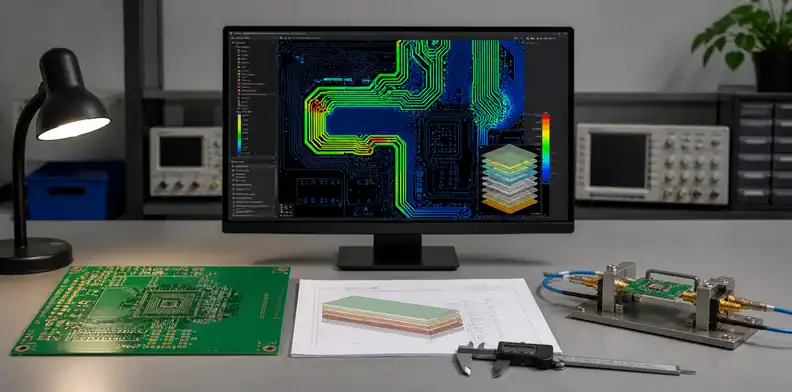
Quick Answer: AI PCB impedance stackup control is not created by drawing a trace and seeing a clean rule result. Controlled impedance needs a target value, routing layer, return plane, dielectric thickness, laminate Dk, finished copper, trace geometry, tolerance, and measurement method. Code can propose geometry, but the fabricator must turn that geometry into a buildable stackup.
Code-generated boards often treat impedance as a routing value. Manufacturing treats it as a stackup, material, lamination, and measurement decision. This article separates the engineer’s responsibility from the fabricator’s stackup calculation and TDR evidence.
Table of Contents
- Does a code-generated board control impedance?
- Is there one correct 50 ohm trace width?
- Who owns the stackup decision?
- Why can a green checkmark mislead designers?
- What tolerance and evidence should be requested?
- How should the RFQ specify impedance?
- How is impedance verified after fabrication?
- When should the design be rerouted?
- What happens when the fabricator changes geometry?
- How should impedance changes be approved?
Does a code-generated board control impedance?
No. Keep the impedance note inside the AI-generated PCB release checklist whenever geometry, stackup, material, tolerance, and verification must be frozen with the same order package.
A script can draw a 50 ohm trace width based on assumed FR-4 and dielectric height. If the supplier builds a different dielectric thickness or copper foil, the finished impedance can shift even though the layout still looks correct.
For a scripted 50 ohm trace, record the assumed dielectric height, copper thickness, solder mask condition, and material Dk used by the calculator. The practical reason is that the number is not portable when any of those inputs changes.
For a scripted 50 ohm trace, record the material family, dielectric height, copper thickness, reference plane, and solver assumption used for the width.
Impedance rule: A trace width is only controlled after the stackup and test method are part of the quote.
Is there one correct 50 ohm trace width?
No. The width depends on routing layer, return path, dielectric spacing, laminate Dk, finished copper, solder mask condition, and target tolerance.
A 50 ohm microstrip, 90 ohm USB differential pair, and 100 ohm Ethernet pair can need different geometries on the same board. Moving from outer to inner layers changes the field structure and the answer.
For a differential-pair interface, state whether the target is single-ended, differential, or both, and name the interface when useful. The practical reason is that the fabricator cannot infer USB, Ethernet, RF, or clock intent from width alone.
For a differential-pair interface, preserve pair spacing, intra-pair skew target, reference layer, and connector launch geometry in the stackup note.
Controlled impedance inputs:
| Input | Why it matters | Owner |
|---|---|---|
| Target value | Defines electrical goal | Engineering |
| Dk and dielectric height | Sets geometry | Fabricator |
| Copper thickness | Changes finished width | Fabricator |
| TDR coupon | Provides evidence | Both |
There is no single 50 ohm number that survives a material or layer change. The answer shifts with resin content, glass style, copper thickness after plating, trace shape after etching, solder mask coverage, and distance to the reference plane. A code-generated rule can be a starting calculation, but the fabricator still needs the actual material system and finished copper assumptions before the width is released.
Who owns the stackup decision?
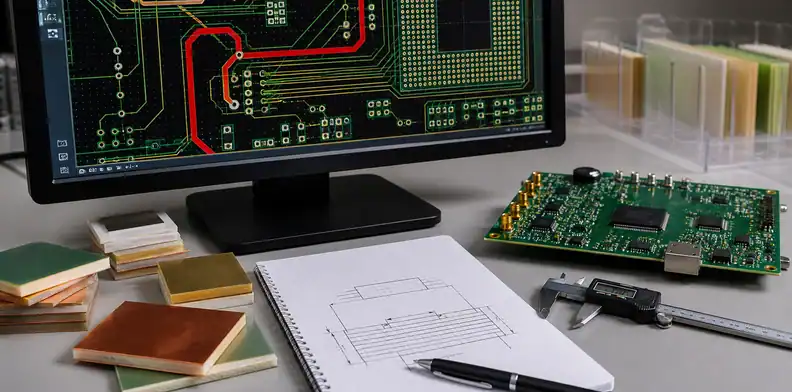
Engineering owns the electrical target; the fabricator owns the manufacturable stackup proposal.
The buyer should state target impedance, net class, layer preference, tolerance, and whether TDR coupons are required. The fabricator should return dielectric thickness, material family, copper weight, predicted geometry, and tolerance limits.
For a fabricator stackup proposal, compare predicted geometry with the routed clearance before engineering signs off. A technically correct stackup can still force rerouting when the AI design used too little room.
If the fabricator proposes a different stackup, return the material, dielectric, copper, and impedance deltas to engineering before file release.
Owner boundary: Supplier geometry changes need engineering approval when they affect high-speed performance.
Ownership should be split clearly: engineering owns the electrical target, the fabricator owns buildable material options, and purchasing owns the record that joins those two decisions. If a supplier proposes another prepreg, core, copper foil, or dielectric thickness, the change should return to engineering before the quote is locked. Otherwise the final board may meet fabrication convenience while missing the original signal budget.
Why can a green checkmark mislead designers?
A rule check can verify width and spacing while ignoring the material model behind the trace. The companion PCB DRC vs DFM limits article explains why a green rule report can still miss a fabrication constraint.
AI and code tools often assume Dk near 4.2 to 4.5 for generic FR-4, but real laminate, resin content, glass weave, and frequency behavior change the result. The CAD file may also ignore solder mask effect on outer layers.
For a generic FR-4 assumption, ask whether the material model matches the quoted laminate and frequency range. The practical reason is that Dk variation can move impedance even when copper geometry is unchanged.
For a generic FR-4 assumption, ask for the actual laminate, resin content, copper finish, and Dk used in the impedance model.
What tolerance and evidence should be requested?
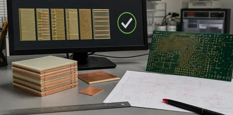
State the target and acceptable range, then define coupon or board-level TDR evidence.
Common targets such as 50 ohm single-ended, 90 ohm USB differential, and 100 ohm differential pairs are not complete specifications without tolerance. Many commercial builds use a tolerance such as +/-10%, but tighter or looser values depend on design risk and supplier process.
For a coupon requirement, decide before panelization whether impedance evidence must be measured or only calculated. The practical reason is that TDR coupons need planning and cannot be added after the panel is full.
When a coupon requirement appears, add the coupon style and measurement expectation to the drawing or procurement note before ordering.
Example target classes:
| Interface | Typical target | Release note |
|---|---|---|
| RF/single-ended | 50 ohm | Layer and reference plane |
| USB differential | 90 ohm | Pair spacing and tolerance |
| Ethernet differential | 100 ohm | Coupon requirement |
| Clock line | Project-specific | Length and layer control |
Proof rule: The RFQ should say whether predicted impedance is enough or whether TDR evidence is required.
For controlled impedance, ask how the tolerance will be verified rather than only asking for a percentage. Useful evidence can include the coupon design, coupon location, test method, measured trace type, layer pair, and whether the report gives actual values or only pass/fail status. That level of detail matters when a later issue appears on one net class but not another.
How should the RFQ specify impedance?
List controlled nets, layers, reference planes, target values, tolerance, and whether geometry may change.
Attach the stackup proposal or ask the fabricator to return one before order release. Do not bury impedance in a screenshot or a chat note; it belongs in the fabrication notes, stackup table, or quote request.
For an impedance note in the drawing, list layer, reference plane, target value, tolerance, and controlled nets in one place. The practical reason is that a buried note or screenshot is easy to miss during CAM review.
For an impedance note, store the target ohms, net class, layer pair, tolerance, and test coupon reference with the drawing.
A good impedance RFQ names each controlled net class, target value, tolerance, reference layer, and whether the target applies before or after solder mask. It should also state whether the buyer expects the supplier to propose stackup changes or only confirm the released stackup. That difference matters because one path invites engineering review, while the other treats the released geometry as fixed.
How is impedance verified after fabrication?
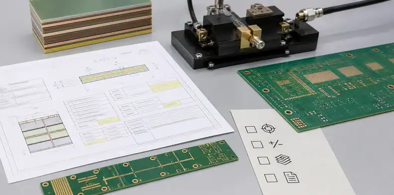
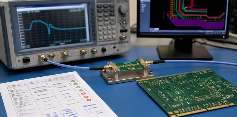
Verification usually uses a test coupon and TDR measurement matched to the panel and stackup. Use AI PCB manufacturing evidence when coupon records, layer identity, and measured values must be tied to the finished lot.
The coupon should represent the controlled layers and geometries. If there is no coupon or measurement plan, acceptance rests on calculation and process control only, which may be acceptable for low-risk boards but weak for high-speed interfaces.
For a measured TDR result, compare the result with the agreed tolerance and the specific coupon geometry. The practical reason is that a measurement without target, tolerance, and location is hard to accept or reject.
Close a measured TDR result by keeping actual ohms, coupon identifier, layer pair, and test date beside the stackup release.
TDR check: Decide the evidence level before production because coupons cannot be added after the panel is built.
When should the design be rerouted?
Reroute when the fabricator’s stackup requires geometry that no longer fits the board or the design margin.
Supplier feedback may change trace width, spacing, via transitions, reference-plane assignment, or layer selection. For dense AI-routed boards, accepting the impedance stackup may require moving parts or rerouting critical nets.
For a supplier geometry change, treat changes to controlled traces as engineering changes, not routine CAM cleanup. The practical reason is that the board may still fabricate while the signal target has shifted.
A supplier geometry change is controlled when engineering approves the trace or dielectric change and TDR evidence is defined.
Rerouting is usually cleaner than forcing the fabricator to chase an impossible stackup. If the approved material set cannot support the target width, spacing, or reference plane without hurting yield, update the trace geometry and release a new layout. That avoids a hidden manufacturing correction that only appears after CAM asks for wider traces or different dielectric height.
What happens when the fabricator changes geometry?
A geometry change should be treated as an engineering decision when the net is controlled.
The fabricator may widen, narrow, or move controlled traces to meet the stackup target. That can be correct, but it can also change routing clearance, coupling, length matching, or component escape. Ask for the proposed stackup and finished geometry before approving production so the electrical owner can judge the change.
Change rule: CAM may propose impedance geometry, but engineering should approve it before the build.
Geometry changes should be returned as a marked stackup or CAM note, not buried inside a quote comment. Ask the supplier to identify the layer, original width or spacing, proposed value, material assumption, and verification method. If the change affects more than one impedance class, engineering should approve the combined effect rather than approving each trace in isolation.
How should impedance changes be approved?
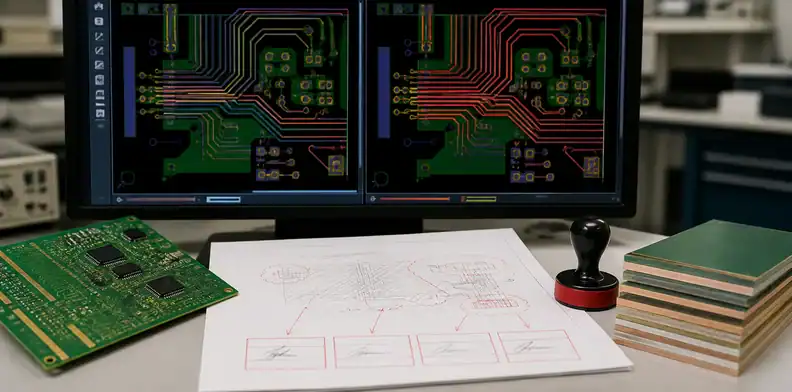
Approve impedance changes through a named stackup revision and a measurement or calculation basis.
The approval should state target value, tolerance, controlled layers, affected nets, proposed width/spacing, material, copper weight, and whether TDR evidence is required. Without those fields, the same design can be quoted as ordinary routing by one supplier and controlled impedance by another.
Approval rule: Controlled impedance approval needs stackup data, not only a note saying 50 ohm.
For quote comparison, separate ordinary routing from controlled impedance scope. A supplier who calculates a stackup, changes geometry, builds a coupon, and provides TDR evidence is not quoting the same work as a supplier who only fabricates the artwork. Put those assumptions into the RFQ table so purchasing can compare scope instead of treating the lowest upload price as an equivalent offer.
The safest readback after CAM review is a small impedance disposition: accepted target, accepted stackup, final width and spacing, controlled layers, coupon or no-coupon decision, and who approved any geometry change. That record helps the next revision because a code-generated board may regenerate traces from old assumptions unless the approved manufacturing stackup is fed back into the design rules.
For stackup review, send QueenEMS the impedance table, stackup drawing, material preference, copper weights, coupon request, and solver assumptions through the QueenEMS contact page. Note the target values, tolerance, quantity, and supplier geometry changes that require engineering approval.
FAQ
Can AI calculate the right impedance trace?
Only as a starting estimate. The final answer must use the fabricator’s stackup, material, copper, and verification plan.
Do I need TDR for every PCB?
No. Use TDR when impedance is a real acceptance requirement or when the interface risk justifies coupon evidence.
Can the fabricator change trace width for impedance?
Yes, if engineering approves the change and the updated geometry still fits the routing and performance requirements.
What’s the best way to approve an impedance stackup change?
The best approval is a named engineering release that freezes dielectric thickness, copper weight, trace geometry, coupon plan, and measurement method. Verbal approval is weak because the fabricator may need to adjust more than one variable to hit the impedance target.
Sources
Written by the QueenEMS Engineering Team
Upload your files today · Free DFM check before production · Ship worldwide
Get your PCB prototypes in as fast as 24 hours. We handle FR4, Rogers, and hybrid boards up to 40 layers in volume production, with advanced builds subject to engineering review — free prototypes for 2–4 layer FR-4 boards, no minimum order.
Just upload your Gerber + BOM — we source every part, assemble, and inspect (AOI + X‑Ray) so you don't have to chase suppliers. Boards ship in as fast as 24 hours.