
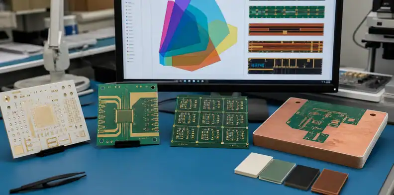
Quick Answer: AI PCB specialty limits appear when a generated board leaves standard FR-4 assumptions. Ceramic, RF, HDI, BT substrate, heavy copper, and high-voltage designs need material data, stackup rules, process limits, and evidence that generic AI routing rarely knows. The practical choice is to re-engineer the file in a specialty process path or keep the AI design as a concept only.
Standard FR-4 workflows hide many assumptions that are not portable to specialty boards. The board outline may survive, but impedance, via structure, material behavior, and copper rules can change completely. This article is a conversion-focused spoke for deciding when AI output needs specialty fabrication review before quote.
Table of Contents
- Can AI tools handle specialty PCB requirements?
- Where do FR-4 assumptions fail first?
- Can AI design ceramic or BT substrate boards?
- What changes for RF and high-frequency boards?
- Where do HDI and microvias break assumptions?
- How does heavy copper change design limits?
- Should you redraw or ask the fab to re-engineer?
- What should a specialty quote package include?
- How do lead time and cost assumptions change?
- What evidence should close the specialty quote?
Can AI tools handle specialty PCB requirements?
Only when the specialty material and process limits are deliberately modeled. Most AI board generation workflows are trained around common FR-4 rules, simple layer counts, and commodity prototype constraints. The AI-generated PCB release checklist keeps the specialty review connected to the larger RFQ package. They do not automatically understand ceramic shrinkage, RF laminate handling, microvia reliability, BT substrate rules, or heavy-copper spacing.
For an AI layout outside FR-4 defaults, identify the board family before trusting line, via, stackup, or material assumptions. The practical reason is that a file that looks complete can belong to the wrong process world.
For a layout outside FR-4 defaults, make the material family, process class, and supplier capability check visible before the drawing is priced.
Specialty rule: Treat AI output as a concept until the specialty process owner reviews material and build limits.
Where do FR-4 assumptions fail first?
They fail at material properties, stackup, drilling, copper behavior, and verification evidence.
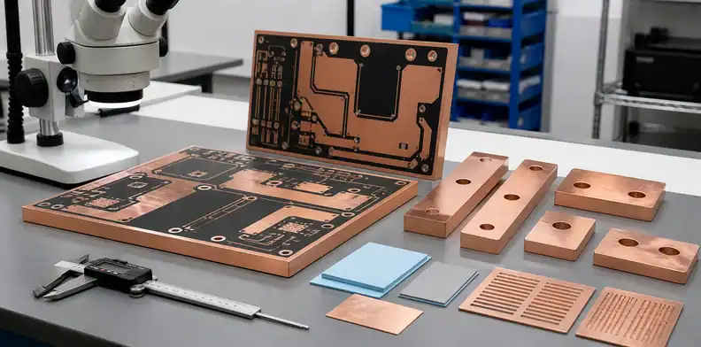
Ceramic substrates can have Dk near 9 rather than FR-4 values near 4.2 to 4.8. RF materials may need controlled dielectric behavior and copper roughness choices. Heavy copper above 3 oz changes trace spacing and thermal decisions.
For a ceramic or RF material, compare Dk, thickness, copper, and thermal path against the actual substrate. The practical reason is that material behavior changes the electrical and thermal answer.
For ceramic or RF material, record the laminate or substrate grade, thickness, copper profile, and any supplier-proposed substitute for engineering approval.
Specialty board decision map:
| Board type | AI blind spot | Required review |
|---|---|---|
| Ceramic | Dk and thermal path | Substrate process |
| RF | Loss and launch | Impedance stackup |
| HDI | Microvia sequence | Lamination plan |
| Heavy copper | Etch and spacing | Copper process |
FR-4 assumptions fail when the material behavior drives the process rather than the routing grid. Ceramic shrinkage, PTFE handling, BT substrate drilling, high-Tg laminate choice, and heavy-copper etching all change the supplier’s normal limits. If the AI output uses commodity trace spacing, via sizes, or stackup defaults, ask the supplier to confirm the specialty material before treating the layout as buildable.
Can AI design ceramic or BT substrate boards?
It can draw geometry, but it usually cannot finish the manufacturing decision.
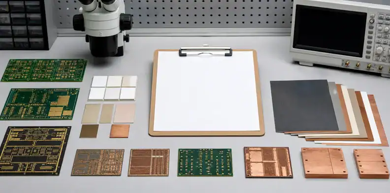
Ceramic and BT boards depend on substrate thickness, metallization, thermal path, pad finish, panel size, and supplier-specific process rules. A generated file may need a specialty stackup and layout pass before quotation.
For a ceramic or BT quote, send substrate target, metallization need, finish, and thermal requirement with the generated files. The practical reason is that a standard board quote form may miss the real cost driver.
When ceramic or BT assumptions change, revise the material callout, thickness target, and panel handling note before supplier review continues.
Substrate call: Ask for material review before treating an AI-drawn ceramic or BT board as a build file.
What changes for RF and high-frequency boards?
RF boards need material, stackup, launch, impedance, and loss decisions that generic routing does not solve. For RF stackup limits, code-generated PCB stackup control gives the adjacent impedance-release workflow.
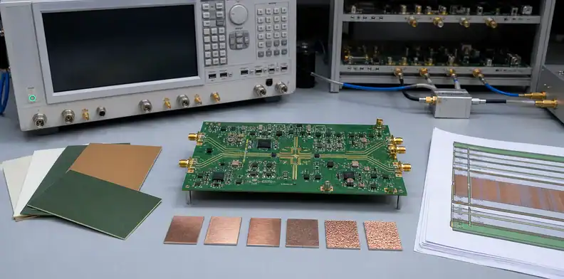
Line width, copper roughness, solder mask, reference-plane continuity, via transitions, and connector launch shape affect RF behavior. A visually neat AI route can still be electrically wrong.
For an RF launch area, review connector launch, reference plane, via transition, and solder mask treatment as a local RF structure. The practical reason is that autorouting can make a neat connection that performs poorly.
For an RF launch area, confirm laminate, launch geometry, mask opening, connector footprint, and nearby copper keepout before quote approval.
RF review needs more than a controlled-impedance number. The stackup should show laminate family, dielectric thickness, copper roughness assumptions, reference planes, launch geometry, keepouts, and any solder mask decision over the RF path. A supplier may be able to build the geometry, but engineering still has to decide whether the proposed material and copper profile fit the loss and phase budget.
Where do HDI and microvias break assumptions?
HDI requires sequential lamination, microvia stack rules, pad size control, and reliability review.
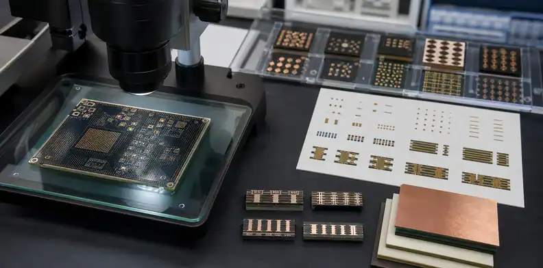
AI tools may place via structures that look compact but conflict with build sequence, aspect ratio, capture pad, fill, or stacked-via reliability. The cost and yield path changes quickly when blind or buried vias enter the design.
For an HDI via stack, define blind, buried, stacked, or staggered via intent before the supplier prices lamination. The practical reason is that HDI cost and reliability depend on sequence, not only density.
If the HDI stack changes, update the lamination sequence, microvia type, capture pad, and fill requirement as a package.
Redraw vs re-engineer:
| Situation | Likely action | Reason |
|---|---|---|
| Minor clearance issue | CAM/DFM feedback | No intent change |
| Wrong material model | Engineering rewrite | Electrical result changes |
| Invalid via stack | HDI redesign | Build sequence changes |
| Heavy copper upgrade | Rule reroute | Spacing changes |
HDI check: Define via structure and lamination sequence before accepting the generated routing.
HDI risk depends on via structure, layer transition, dielectric thickness, capture pad, copper fill, and whether vias are stacked, staggered, or skipped. A generic AI router may place dense fanout that looks reasonable on screen but needs a sequential lamination plan. The quote request should separate what is required by the component escape from what can be changed for yield.
How does heavy copper change design limits?
Heavy copper increases spacing, etch compensation, thermal behavior, and fabrication difficulty.
A 3 oz or 4 oz copper feature cannot be treated like a thin signal layer. Trace width, isolation, solder mask, plating, and heat distribution need different rules, and finished geometry may diverge more from artwork.
For a heavy-copper upgrade, reroute spacing and thermal features for the target copper weight instead of upgrading after layout. The practical reason is that finished copper behavior changes with thickness.
For heavy-copper upgrades, record copper weight per layer, clearance relief, plating concern, and DFM approval owner.
Heavy copper changes etch compensation, spacing, solder mask relief, thermal balance, drill-to-copper clearance, and plating expectations. The same current path that solves an electrical requirement can create a fabrication issue if copper density is not balanced. Ask for a DFM review that names the copper weight per layer and any area where the supplier needs relief, thieving, or outline adjustment.
Should you redraw or ask the fab to re-engineer?
Use the AI file as a concept when material or process assumptions are wrong.
For minor DFM edits, supplier CAM feedback may be enough. For ceramic, RF, HDI, BT, or heavy copper, expect a specialty engineering pass that may change stackup, copper geometry, via structure, and panel approach.
For a re-engineering decision, decide whether the AI file is a concept, a partial layout, or a release candidate. The practical reason is that the answer controls how much specialty engineering is needed.
Close a specialty re-engineering decision by recording which geometry may change and which RF, HDI, ceramic, or copper requirement is fixed.
Decision rule: Re-engineer when the process changes the electrical or thermal design, not only the file format.
Redraw when the specialty requirement changes the electrical or mechanical intent, such as an RF launch, microvia stack, current path, or ceramic shrinkage allowance. Ask the fabricator to re-engineer only within a bounded decision, such as panelization, copper relief, manufacturable spacing, or material availability. The quote should make that boundary visible so CAM does not redesign a performance feature without approval.
What should a specialty quote package include?
Send the generated files plus material target, stackup need, electrical or thermal goal, evidence requirement, and acceptable changes.
Use PCB material substitution approval when the supplier proposes laminate or substrate alternatives. For QueenEMS review, attach the AI output and state which specialty board type is required before the quote is compared.
For a specialty RFQ, state the evidence that should close the process risk, such as coupon, microsection, impedance report, or material approval. The practical reason is that specialty quotes need acceptance proof as much as price.
A specialty RFQ is controlled when material, process class, supplier limits, and engineering approval boundaries are clear before pricing.
How do lead time and cost assumptions change?
Specialty boards change price and lead time through material, process sequence, yield risk, and evidence scope.
Ceramic, RF laminate, HDI lamination, BT substrate, and heavy copper are not priced like standard FR-4 prototypes. Material availability, panel size, drilling method, plating route, controlled impedance, microsection, or coupon evidence can drive both cost and schedule. A fast AI concept does not shorten those physical constraints.
Quote rule: Specialty cost comparison should include process family, material, yield risk, and evidence scope.
Specialty boards often carry cost and lead-time risk from material availability, coupon needs, sequential lamination, controlled drilling, plating burden, or extra inspection. The buyer should ask which item drives the quote instead of assuming the premium is only board area or layer count. That answer helps decide whether to simplify the design, approve a substitute material, or keep the specialty requirement.
What evidence should close the specialty quote?
Close the quote with the evidence that proves the specialty feature was actually controlled.
For RF, that may be stackup and impedance evidence. For ceramic, it may be substrate and metallization approval. For HDI, it may be microvia structure evidence. For heavy copper, it may be cross-section or spacing confirmation. The evidence should match the feature that made the board specialty in the first place.
Evidence rule: Specialty acceptance proof should follow the specialty risk, not a generic report list.
Specialty-board review should start before the AI file is cleaned for fabrication. If the material family changes, the board may need different copper rules, different via structures, different panel assumptions, and different evidence. Asking a specialty fabricator to quote after a standard FR-4 autoroute can force them either to reject the package or rebuild the engineering logic from scratch.
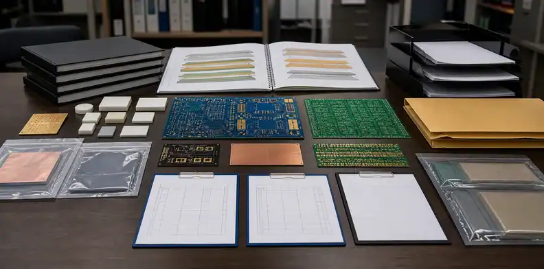
A useful buyer readback classifies the AI file as concept, partial release, or build candidate. Concept means the file communicates placement and intent. Partial release means some geometry is usable but stackup or material work remains. Build candidate means the specialty process owner has reviewed material, stackup, feature limits, and evidence. Without that classification, the quote discussion mixes design service and fabrication pricing.
For specialty PCB review, send QueenEMS the material callout, stackup, copper weight, via structure, RF or ceramic constraints, evidence request, and build quantity through the QueenEMS contact page. Separate supplier-adjustable geometry from performance requirements that engineering must approve.
FAQ
Can AI create a ceramic PCB layout?
It can create a layout concept, but ceramic material and process rules still need specialty engineering review.
Can a standard FR-4 AI design become HDI later?
Sometimes, but microvia structure, pad size, layer sequence, and cost usually require rerouting.
What is the safest way to quote an AI specialty PCB?
Send the AI files with material, stackup, impedance, thermal, via, copper, and evidence requirements clearly stated.
Can I quote a specialty PCB from standard FR-4 AI rules?
No, standard FR-4 rules are only a starting point because ceramic, RF, HDI, heavy copper, and high-temperature boards use different materials, tolerances, and process controls. The quote package should state the specialty constraint first, then let the supplier confirm whether the layout is buildable.
Sources
Written by the QueenEMS Engineering Team
Upload your files today · Free DFM check before production · Ship worldwide
Get your PCB prototypes in as fast as 24 hours. We handle FR4, Rogers, and hybrid boards up to 40 layers in volume production, with advanced builds subject to engineering review — free prototypes for 2–4 layer FR-4 boards, no minimum order.
Just upload your Gerber + BOM — we source every part, assemble, and inspect (AOI + X‑Ray) so you don't have to chase suppliers. Boards ship in as fast as 24 hours.