
Most failures in high-frequency boards trace back to poor PCB antenna design, where a single 0.05mm stackup deviation drops RF range by 50%. You spend weeks perfecting the schematic, but when the prototype arrives, the BLE range is barely 10 meters instead of 50 meters. This happens because reference designs fail to account for specific fabrication variables, resulting in massive signal reflection. As an experienced RF PCB manufacturer, we catch these exact errors daily on the production floor. In this guide, we break down the seven most expensive manufacturing mistakes and provide exact factory data to fix them.
Quick Answer: Most PCB antenna design failures trace back to seven recurring mistakes: copying reference designs without re-tuning, undersized ground planes (below 80mm at 2.4 GHz), poor 50-ohm matching (S11 worse than -10 dB), wrong substrate above 3 GHz, ignoring enclosure detuning (1–2% frequency shift from plastic alone), loose manufacturing tolerance (±50μm vs the ±25μm RF needs), and skipping VNA/OTA validation. Each mistake costs 10–30% range or causes redesign cycles of $5,000+. Key takeaways:
- Trace width tolerance of ±25μm shifts antenna frequency by 2–3%
- Ground plane under 80mm at 2.4 GHz drops effective range by 30%+
- Plastic enclosures shift resonance 1–2%; metal blocks signal entirely
- $50–150 NanoVNA replaces $5,000+ VNA for prototype validation
Table of Contents
- What Are the Most Costly PCB Antenna Design Mistakes?
- Mistake #1: Copying Reference Designs Without Adjusting for Your Stackup
- Mistake #2: Undersized Ground Plane That Kills Your Signal
- Mistake #3: Ignoring 50-Ohm Impedance Matching in PCB Antenna Design
- Mistake #4: Using Standard FR4 Above 3 GHz
- Mistake #5: Forgetting Enclosure Detuning Until Final Assembly
- Mistake #6: Skipping Manufacturing Tolerance Specs (±25μm Matters)
- Mistake #7: Validating Without VNA or OTA Testing
- How to Choose Materials That Avoid These PCB Antenna Design Errors?
- How to Pick a Manufacturer That Catches These PCB Antenna Design Mistakes?
What Are the Most Costly PCB Antenna Design Mistakes?
The most costly mistakes in PCB antenna design involve mismatched stackups, undersized ground planes (under 80mm), and ignoring enclosure detuning, which collectively cause up to 80% of signal loss. When you skip RF-specific design rules, your board fails certification and requires expensive redesign cycles. Identifying these specific errors before releasing Gerber files saves thousands of dollars in wasted prototype runs.
How Do Different Antenna Types Compare?
Every wireless product requires a specific antenna architecture based on space constraints and frequency targets. Choosing the wrong type upfront restricts your layout options permanently.
Let’s look at the options:
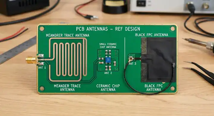
- Trace Antennas: Printed directly on the PCB copper layer. They cost nothing extra but require massive board space.
- Chip Antennas: Ceramic surface-mount components. They save physical space but demand precise ground plane sizing.
- Flex (FPC) Antennas: Standalone flexible circuits connected via a cable. They bypass PCB ground plane issues entirely.
Why Does the Ground Plane Act as Half the Antenna?
The ground plane acts as the counterpoise, providing the return path for the RF currents radiating from the physical antenna element. Without it, the antenna cannot form a complete dipole, resulting in severe performance drops.
Here is what happens in reality:
- The ground plane dictates the radiation pattern and efficiency.
- Cutting the ground plane in half reduces the radiated power by more than 50%.
- A fragmented ground plane creates parasitic inductance, shifting the center frequency.
The 7 Mistakes Overview
Understanding the cost and severity of these mistakes helps you prioritize your design reviews. Here is the full breakdown of the errors we see constantly on the factory floor.
Bottom line: Failing to address these seven manufacturing mistakes early forces you into reactive debugging, adding $5,000+ and weeks of delay to your product launch.
| Mistake Name | Consequence | Severity Level | Typical Fix Cost |
|---|---|---|---|
| Copied Reference Design | 55-58 ohm mismatch | High | $1,500 (Redesign) |
| Undersized Ground Plane | 30%+ range drop | Critical | $3,000 (Board resize) |
| Poor 50-Ohm Matching | S11 > -10 dB | High | $500 (Component tuning) |
| FR4 above 3 GHz | Massive attenuation | Critical | $2,000 (Substrate swap) |
| Enclosure Detuning | 1-2% frequency shift | High | $4,000 (Tooling change) |
| Loose Tolerance (±50μm) | Batch-to-batch yield drops | Medium | Per-batch tuning labor |
| No VNA/OTA Validation | Blind field failures | Critical | $10,000+ (Product recall) |
Mistake #1: Copying Reference Designs Without Adjusting for Your Stackup
Copying a reference design directly fails because your fabricator’s prepreg thickness usually differs from the original by 0.05mm to 0.15mm, shifting your 50-ohm trace to 55-58 ohms. This physical mismatch ruins the targeted impedance, drastically reducing the transmission range.
Why Did My Copied TI Antenna Fail?
You might be asking the same question we saw on the TI E2E Forum: “I copied an inverted-F antenna directly from the TI reference design but my range is half of theirs. I followed the dimensions exactly. Why?”
Here is the exact reason:
- The reference design likely used a 1.6mm board thickness (actual 1.55-1.62mm).
- Your specific fabrication process might yield a 1.5mm board (actual 1.45-1.55mm).
- That tiny 0.05-0.15mm difference pushes the trace impedance off the 50-ohm target.
- Your S11 drops from the designed -15 dB to a dismal -5 to -7 dB, reducing your range by 30-50%.
How Do You Adjust for Manufacturing Reality?
To fix this, you must request the actual stackup values from your manufacturer before routing the board. Per Texas Instruments’ application note SLOA241C, maintaining at least 10mm spacing between the ground plane and antenna coil minimizes inductance impact and detuning. You then recalculate the trace width based on the factory’s specific dielectric constant (Dk) and prepreg thickness.
Bottom line: Never reuse a reference trace width without recalculating it against your specific factory’s impedance test coupon report.
Mistake #2: Undersized Ground Plane That Kills Your Signal
An undersized ground plane acts as a choked counterpoise, dropping your antenna efficiency by 5 to 8 dB and reducing your effective range by over 30%. Because the ground plane functions as the lower half of the antenna structure, restricting its size physically prevents the RF wave from propagating properly.
Can I Use a 30x30mm Board for 2.4 GHz?
A common struggle on the EEVBlog Forum perfectly highlights this issue: “I have a tiny 30x30mm board for my BLE wearable. Is that enough ground plane for the chip antenna at 2.4 GHz? Do I really need 80mm?”
The harsh reality is no:
- The quarter-wavelength at 2.4 GHz is 31mm, which represents the absolute minimum, not “enough.”
- The ideal ground plane size for a 2.4 GHz chip antenna is ≥80mm × 40mm.
- Shrinking from 80mm to 30mm causes a 5-8 dB efficiency drop, which equals 75-85% energy loss.
- For 433 MHz, the situation is worse; the ideal ground is ≥170mm, making a 30mm board barely functional.
What Are the Workarounds for Small Devices?
When mechanical constraints prevent an 80mm board, you must look outside the main PCB. One solution is using the metal parts of the product enclosure as a ground extension. Alternatively, you can contact a flexible PCB manufacturer to design an FPC antenna, because FPC antennas have built-in ground planes that do not rely heavily on the host PCB.
Bottom line: If your board cannot accommodate an 80mm ground plane, you must switch to an off-board antenna solution to maintain a reliable connection.
| Ground Plane Size (2.4 GHz) | Efficiency Loss | Radiated Power | Recommendation |
|---|---|---|---|
| ≥80mm × 40mm | 0 dB | 100% | Ideal target |
| 50mm × 30mm | -3 dB | 50% | Acceptable for short range |
| 30mm × 30mm | -5 to -8 dB | 15-25% | Requires redesign/FPC |
Mistake #3: Ignoring 50-Ohm Impedance Matching in PCB Antenna Design
Ignoring 50-ohm impedance matching reflects up to 60% of your power back to the transmitter, indicated by an S11 worse than -10 dB. When the trace impedance does not match the antenna and transceiver, the resulting standing waves severely degrade the signal quality. For standard tuning practices, consult our controlled impedance PCB design guide to hit the right trace widths before assembling components.
What Should I Tune First When S11 is Bad?
We see engineers panic over bad matching, much like this Reddit r/AskElectronics user: “My S11 is only -4 dB at 2.45 GHz. What should I tune first—the matching network components or the antenna trace length?” S11 = -4 dB means 60% of energy is reflecting, which is far below the -10 dB standard.
Follow this strict debugging order:
- First, verify all layers in the keep-out zone are completely clear of copper (this fixes 80% of issues).
- Second, verify the trace width is actually 50 ohms based on the factory’s stackup report.
- Finally, adjust the matching network components.
How Factory Prepreg Deviations Ruin Matching
During a small batch run for an IoT gateway client, the initial S11 was only -5 dB instead of the -15 dB target. Our engineers pulled the Gerber files and discovered their stackup assumed a 0.2mm prepreg, but the prototype fab used 0.18mm. This 10% deviation shifted the 50-ohm trace to 55-ohm. By recalculating the trace width from 11 mil to 12.5 mil on the same stackup, the S11 improved to -18 dB, and the field range jumped from 42 meters to 67 meters.
Bottom line: Always tune your keep-out zones and stackup trace widths before blindly swapping capacitors in your Pi-network.

| Matching Network Type | Configuration | Tuning Flexibility | Typical Use Case |
|---|---|---|---|
| Pi-Network | Shunt C, Series L, Shunt C | Very High | Standard for new designs |
| L-Network | Series L, Shunt C | Medium | Space-constrained layouts |
| 0-Ohm Placeholder | Single Series Resistor | Zero | Only for pre-matched ICs |
Mistake #4: Using Standard FR4 Above 3 GHz
Using standard FR4 above 3 GHz causes massive signal attenuation because its high loss tangent (0.02) and unstable dielectric constant heavily absorb and detune high-frequency signals. Standard FR4 performs adequately for 2.4 GHz Wi-Fi, but pushing it into the 5 GHz or 5G bands results in severe thermal dissipation and signal loss.
Why Does Standard FR4 Fail at High Frequencies?
Standard FR4 is a fiberglass-epoxy composite built for mechanical stability, not radio wave propagation. Above 3 GHz, the material properties degrade non-linearly.
Consider these material limits:
- Standard FR4 has a variable Dk that fluctuates ±10% between different factory batches.
- This batch-to-batch fluctuation actively shifts your antenna’s resonant frequency.
- The high dissipation factor converts your transmitter’s power directly into heat.
When Do You Switch to Advanced Substrates?
You must switch to specialized high-frequency materials when working above 3 GHz. Rogers RO4003C or RO4350B provide tight Dk control and low loss tangents, keeping the signal intact up to 10 GHz. For radar or mmWave applications above 24 GHz, PTFE-based substrates become mandatory.
Bottom line: Do not use standard FR4 for designs operating above 3 GHz; the material inconsistencies will ruin your production yields.
| Material | Max Recommended Freq | Loss Tangent | Relative Cost |
|---|---|---|---|
| Standard FR4 | < 3 GHz | ~0.020 | 1x (Baseline) |
| Rogers RO4003C | 2 – 10 GHz | ~0.0027 | 3x to 5x |
| PTFE (Teflon) | > 24 GHz | < 0.001 | 10x+ |
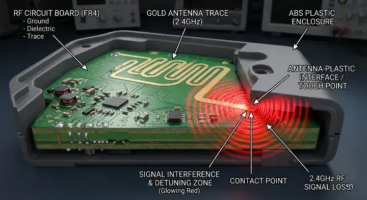
Mistake #5: Forgetting Enclosure Detuning Until Final Assembly
Forgetting enclosure detuning drops your resonant frequency by 1–2% because plastic housings add parasitic capacitance, shifting a 2.4 GHz signal by up to 50 MHz. When an antenna radiates near a physical object, the dielectric material of that object becomes part of the antenna system, resulting in a severe impedance mismatch. According to Microwaves & RF, antenna resonant frequency drops as effective capacitance increases from larger ground planes or thicker plastic enclosures.
Why Does the Case Kill the Signal?
A frustrated user on EDABoard asked: “My antenna was perfectly tuned on a bare board. After putting it in the ABS plastic case, the resonant frequency shifted by 50 MHz. How do I avoid this?”
Here is the physics behind it:
- ABS plastic has a Dk of approximately 2.5 to 3.0.
- When placed flush against the antenna, it introduces a 0.5 to 2% frequency shift.
- For a 2.4 GHz BLE signal, this equates to a 12 to 50 MHz drop, pushing the antenna completely out of band.
- PETG plastic (Dk ~2.7) behaves similarly, while metal completely blocks the radiation.
How to Prevent Enclosure Detuning
You must design the mechanical enclosure with the RF layout in mind. Create a mechanical air gap of 3-5mm between the antenna trace and the plastic casing. Furthermore, always leave unpopulated pads for a matching network on your bare board, and perform your final VNA tuning only after the board is secured inside the final enclosure.
Bottom line: Never tune an antenna on a bare board; always perform final impedance matching with the board fully assembled inside its final plastic casing.
| Enclosure Material | Dk Value | Frequency Shift | Signal Blocking |
|---|---|---|---|
| ABS Plastic | 2.5 – 3.0 | -0.5% to -2.0% | Low |
| Carbon Fiber | Conductive | Severe Detuning | Very High |
| Aluminum/Metal | Conductive | Total Detuning | Complete Block |
Mistake #6: Skipping Manufacturing Tolerance Specs (±25μm Matters)
Skipping manufacturing tolerance specs ruins RF yield because a standard ±50μm trace error shifts the resonant frequency by 2–3%, requiring manual retuning per batch. Standard PCB fabrication allows for wider margins, but high-frequency designs demand absolute physical precision. IPC-6012 specifies controlled impedance tolerance of ±10% as standard, with ±5% available for high-frequency RF applications—a doubling of process precision that directly affects antenna yield. Understand the cost impacts by reviewing standard PCB fabrication tolerances.
How Tolerance Drives Factory Yields
Our standard tolerance for RF boards is trace width ±25μm (compared to ±50μm for standard FR4), and we hold impedance control to ±5% (standard is ±10%). This tight control guarantees that at 2.4 GHz, the frequency shift stays within ±30 MHz. Because of this precision, clients can run global certifications on one matching network without reworking every batch. Last year, we delivered 150,000 BLE boards with a 99.7% first-pass yield, with zero returns for antenna detuning.
What Should You Demand from Your Fab?
When getting quotes, you must specify RF-grade tolerances.
Demand the following:
- Trace width etching tolerance no worse than ±25μm.
- Prepreg thickness variance strictly controlled.
- Impedance test coupon reports delivered with every single batch.
Bottom line: Always specify ±25μm trace tolerance and ±5% impedance control on your RF manufacturing notes to prevent batch-to-batch frequency shifts.
| Specification | Standard FR4 Board | High-Frequency RF Board | Impact on 2.4 GHz |
|---|---|---|---|
| Trace Width Tolerance | ±50μm | ±25μm | 2-3% freq shift vs <1% shift |
| Impedance Control | ±10% | ±5% | Noticeable mismatch vs stable S11 |
| First-Pass Yield (Avg) | 60% – 80% | 95% – 99% | High rework cost vs zero rework |
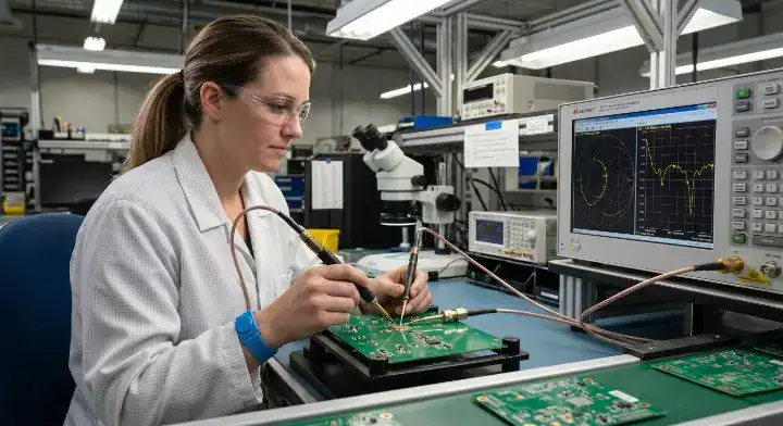
Mistake #7: Validating Without VNA or OTA Testing
Validating without VNA or OTA testing guarantees blind production runs, leading to $5,000+ redesign cycles when field performance inevitably drops. You cannot verify an antenna’s resonant frequency with a standard multimeter; you must measure the reflection coefficient (S11) across the targeted frequency sweep.
How Can Startups Test Without a $10k VNA?
It is a common pain point on Reddit r/PrintedCircuitBoard: “I’m a startup, I don’t have $10k for a Keysight VNA. How do I actually test if my antenna works before shipping?” You do not need a laboratory-grade Keysight machine for basic prototype validation.
- A NanoVNA ($50–150) covers up to 6 GHz, which is perfectly adequate for measuring S11 on 2.4 GHz Wi-Fi or BLE designs.
- For range validation, buy a commercial reference board (like a TI EVM) and perform a fixed-distance RSSI comparison test against your prototype.
- Use a spectrum analyzer in a fixed-distance setup to measure TX power while swapping matching components.
Implementing Factory-Level Testing
For mass production, testing every board in an anechoic chamber ($20k+ to build) is unnecessary. Instead, create a “golden board” that performs perfectly. We use this golden board to build a pogo-pin test fixture that verifies the TX power of every production unit on the assembly line in seconds.
Bottom line: Buy a $50 NanoVNA to measure S11 during prototyping, and use a golden board comparison for mass production line testing.
| Test Equipment | Average Cost | Best Use Case | Capability |
|---|---|---|---|
| NanoVNA | $50 – $150 | Startup Prototyping | Measures S11 up to 6 GHz |
| Spectrum Analyzer | $1,000 – $3,000 | Advanced Tuning | Measures TX power & harmonics |
| Anechoic Chamber | $20,000+ | Final Certification | Perfect OTA radiation patterns |
How to Choose Materials That Avoid These PCB Antenna Design Errors?
Choosing materials to avoid PCB antenna design errors requires matching the substrate’s loss tangent and Dk stability to your exact operating frequency to prevent 30% power dissipation. A perfectly calculated antenna trace will still fail if the underlying fiberglass weaves absorb the RF energy.
Understanding Dielectric Constant (Dk) Stability
The dielectric constant directly dictates the speed at which the RF signal travels through the board.
You need to evaluate materials based on:
- Dk stability across temperature variations (FR4 shifts heavily under heat).
- Moisture absorption rates, because water has a high Dk and ruins tuning in humid environments.
- The fiberglass weave style, because loose weaves cause micro-variations in impedance along the trace length.
Substrate Matching Matrix
Different frequencies demand different structural properties. Using Rogers material for a 433 MHz board is a waste of money, but using FR4 for a 24 GHz automotive radar guarantees total failure.
Bottom line: Lock in your substrate material’s specific Dk value before calculating your trace widths, and never let your fabricator substitute it without permission.
| Frequency Band | Recommended Substrate | Primary Advantage | Cost Profile |
|---|---|---|---|
| < 1 GHz (Sub-GHz) | Standard FR4 | Mechanically strong | Low |
| 1 – 3 GHz (BLE/Wi-Fi) | High-Tg FR4 | Better thermal stability | Low-Medium |
| 3 – 10 GHz (5G/UWB) | Rogers 4350B | Extremely stable Dk | High |
How to Pick a Manufacturer That Catches These PCB Antenna Design Mistakes?
Picking a manufacturer that catches PCB antenna design mistakes means selecting a partner who demands 3D enclosure files and verifies stackup impedances before printing a single board. Standard SMT factories simply print the Gerber files as-is, which means they will blindly manufacture your untuned antenna and charge you for the useless boards.
Why Enclosure Context Matters to the Fab
A 5G small cell client failed OTA testing three times with another fab before coming to us. The first thing we requested was not the Gerber files, but their enclosure 3D step file. We knew that if a metal enclosure’s cutouts deviate from the antenna by over 5mm, severe detuning occurs. By adjusting the feed line path and adding a stitched via cage before fabrication, the first prototype hit the +2.3 dBi gain target, saving the client 6 weeks of development.
The RF Manufacturer Checklist
You need an assembly partner who understands RF physics, not just solder paste.
Check for these capabilities:
- Do they run automated optical inspection (AOI) specifically looking for keep-out zone violations?
- Do they monitor solder paste thickness closely, knowing excess paste alters the Pi-network values?
- Do they have dedicated VNA test stations on the production line?
Bottom line: Choose a manufacturer that forces you to verify your stackup and enclosure mechanics during the DFM phase, saving you from blind production failures.
| Checklist Item | Standard PCB Fab | Professional RF Fab | Why It Matters |
|---|---|---|---|
| Impedance Control | ±10% | ±5% | Prevents batch frequency shifts |
| Trace Tolerance | ±50μm | ±25μm | Keeps traces exactly at 50 ohms |
| DFM Review | Gerber check only | Stackup & Enclosure review | Catches detuning before printing |
Conclusion
Perfecting your RF layout requires more than following a datasheet; it demands strict control over factory variables. From sizing the ground plane to a minimum of 80mm, to specifying ±25μm trace tolerances, every physical detail directly impacts your transmission range. By addressing enclosure detuning early and verifying your specific stackup impedance, you eliminate the blind guesswork that causes 80% of prototype failures. To stop wasting time on blind prototypes and ensure your boards pass certification the first time, contact us today for a comprehensive RF DFM review.
FAQ
Can I use FR4 for a PCB antenna design at 2.4 GHz? Yes, but only with high-Tg FR4 and tight tolerance control. Standard FR4 has a loss tangent around 0.02 which is acceptable below 3 GHz, but Dk varies ±10% across batches—enough to detune your antenna. Send us your stackup and we’ll verify the actual Dk before you commit to FR4.
How do I know if my ground plane is too small for my PCB antenna? If your ground plane is under 80mm × 40mm at 2.4 GHz, it’s too small. You’ll see this as range below 30m for BLE or asymmetric radiation patterns in OTA tests. Either expand the board, switch to an FPC antenna with built-in ground, or use the enclosure metalwork as a ground extension—we can review your design and recommend the cheapest path.
What’s the best way to tune a PCB antenna without a $10k VNA? A NanoVNA at $50-150 covers up to 6 GHz and is enough for S11 measurement on most consumer designs. For range validation, do comparative testing against a known-good reference board at a fixed distance. Send us your board and we’ll do the OTA validation in our test chamber for free during the DFM review.
How much does manufacturing tolerance affect PCB antenna yield? Tolerance directly drives yield. Standard ±50μm trace width on RF boards produces 60-80% first-pass yield on tuned antennas; tighter ±25μm RF-grade tolerance achieves 95-99%. The cost difference is roughly 15-20%, but it eliminates per-batch matching network rework. Ask us for our RF tolerance spec sheet.
Can I assemble a PCB antenna board the same way as a regular SMT board? No—RF boards need extra process controls. Solder paste thickness affects matching network values, and AOI must verify keep-out zones aren’t bridged. Standard SMT lines may skip these RF-specific checks. Talk to us about our dedicated RF assembly line with VNA-equipped test stations.
Upload your files today · Free DFM check before production · Ship worldwide
Get your PCB prototypes in as fast as 24 hours. We handle FR4, Rogers, and Flex up to 60 layers — free prototypes for 2–4 layer boards, no minimum order.
Just upload your Gerber + BOM — we source every part, assemble, and inspect (AOI + X‑Ray) so you don't have to chase suppliers. Boards ship in as fast as 24 hours.