
As devices shrink and high-speed signal integrity demands escalate, standard surface-mount technology (SMT) eventually hits a physical wall. When both sides of your board are packed with fine-pitch BGAs, shifting passive components into the internal layers isn’t just an option—it becomes the only viable layout strategy. But moving from surface-mount to embedded component PCB manufacturing introduces entirely new variables regarding laser trimming, material tolerances, and panel-level yield. From a factory engineer’s perspective, this guide breaks down the real-world math, material choices, and manufacturing realities of embedded passive technology.
1. What Are Embedded Components in HDI PCB Design?
In High-Density Interconnect (HDI) design, embedded components refer to resistors, capacitors, and occasionally active dies that are formed or placed within the internal layers of a printed circuit board. Unlike SMT, which solders components onto the outer surfaces, embedded passives are typically created using specialized thin-film materials laminated and etched directly into the core or prepreg layers.
A frequent question on electronics engineering forums is: “Can active ICs (not just R/C passives) be embedded in HDI inner layers? I keep seeing references to ’embedded active’ but no one explains how.” Yes, active components (bare IC dies) can be embedded, but it is extremely rare in mass production. Embedded active technology is distinct from ABF-substrate level embedding. It requires specialized fabricators with wafer-level handling capability—globally, fewer than 10 front-line fabs (such as AT&S, TDK, and Schweizer) can do it reliably at production volume. Because the cost premium is typically 5-10× that of equivalent surface-mount, embedded active dies are strictly limited to niche applications like automotive BMS, 5G mmWave modules, and ultra-thin medical implants where size or signal-integrity requirements absolute justify the cost. For 95% of standard commercial designs, embedded passives (resistors and capacitors) remain the practical choice.
2. When Should You Use HDI with Embedded Components vs Surface Mount?
Deciding to use HDI with embedded components should be a calculated financial and engineering decision, not a default preference. You should transition from SMT to embedded components when the cost of additional board area, complex BGA fanouts, or poor signal integrity outweighs the manufacturing premium of embedded materials.
If your design team is already seeing the 7 signals you need HDI, introducing embedded passives is the logical next step for extreme density. It becomes highly economical when you are manufacturing between 5,000 and 50,000 units annually and surface-mount passives are blocking critical routing channels beneath 0.4mm pitch BGAs. The decision also heavily impacts your HDI stackup type selection, as embedding materials require specific dielectric pairings and lamination cycles.
3. How Does Embedded Resistor Technology Work Inside HDI Layers?
Embedded resistor fabrication relies on resistive thin films—primarily Nickel-Chromium (NiCr) or Chromium-Silicon (CrSi) alloys. Brands like OhmegaPly CRM, Ticer TCR, and Gould TCR Foil are standard in the industry. The supply chain compliance and testing methods for these thin films are strictly governed by IPC-4811 Specification for Embedded Resistor Material.
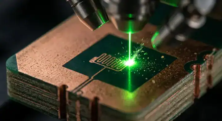
Engineers often ask: “How tight is the tolerance for embedded resistors compared to discrete 0402? Can it actually replace ±1% precision resistors?” The reality is that pre-trim embedded resistors land within a wide ±15% tolerance. After precision laser-trimming, production yield reaches ±2% reliably, and ±1% only under optimal, tightly controlled conditions. It cannot replace ±0.1% precision reference resistors due to the physical limitations of the trimming process. Furthermore, the Temperature Coefficient of Resistance (TCR) is typically ±25-50 ppm/°C for NiCr, which is comparable to an SMT 0402 thin-film’s ±25 ppm/°C. They are best suited for pull-up/pull-down networks, voltage dividers, and terminators.
On our HDI line we run embedded resistor jobs using OhmegaPly CRM30 material — a 25-ohm-per-square nickel-chromium foil laminated to copper. The process is straightforward in concept but unforgiving in execution: pattern-etch the copper layer, etch the resistor pattern, then laminate the inner layer normally. The catch is tolerance. Pre-trim, our embedded resistors land within ±15% of design value about 85% of the time — well outside what most circuits can tolerate. We then laser-trim each resistor to ±2% accuracy using a 1064nm fiber laser, measuring resistance after each cut. This adds roughly 45 minutes of trim time per panel, which is why embedded resistor jobs cost $80-150 more per panel than equivalent surface-mount routing. For a wearable customer running 50,000 units annually, we calculated the trim cost was still cheaper than the BGA fanout space saved by removing 200 discrete 0201 resistors per board. For lower-volume jobs, the math rarely works.
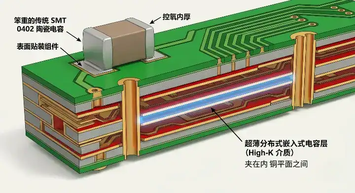
4. How Does Embedded Capacitor Technology Reduce Board Space?
Unlike discrete surface-mount capacitors that take up X-Y real estate, embedded capacitors utilize the Z-axis by acting as distributed capacitance planes. To understand the design frameworks and tolerance expectations for these layers, layout engineers should reference the IPC-2316 Design Guide for Embedded Passive and Active Device Printed Boards.
Embedded capacitors are technically easier than embedded resistors but harder to design with. We work primarily with 3M C-Ply thin-film dielectric — 12μm of high-K material between copper layers gives roughly 8 nF/in² of distributed capacitance. The process is identical to standard inner-layer fabrication: laminate, etch, drill. The difficulty is electrical: embedded capacitor planes are distributed and effective capacitance varies with frequency. Our customers ask for ‘a 100nF decoupling capacitor’ and we have to explain that what they get is approximately 100nF spread across a defined area — the effective ESL is much lower than surface-mount (under 50pH versus 500pH for an 0402), but the tolerance is ±15% versus ±5%. For RF and high-speed digital where you need low impedance from 100MHz to 1GHz, embedded planes outperform discrete capacitors. For tight value-critical filtering, stay with discrete components. About 30% of our embedded component projects use planes only, no discrete bypass at all on the power rails. Other materials like DuPont HK04 thin-film serve similar high-frequency decoupling purposes.
Table: Mainstream Embedded Materials Comparison
| Material Brand | Type | Primary Application | Key Advantage |
|---|---|---|---|
| OhmegaPly CRM30 | Resistor (NiCr) | Pull-up/down, Terminators | Excellent laser trim stability, mature process |
| Ticer TCR | Resistor (NiCr/CrSi) | High-density passive networks | Superior thermal stability and TCR |
| 3M C-Ply | Capacitor | High-speed decoupling | High capacitance density, extreme low ESL |
| DuPont HK04 | Capacitor | RF / Power distribution | Robust dielectric strength, reliable lamination |
5. What Does IPC-7092 Require for HDI Embedded Components?
Adopting HDI with embedded components means adhering to rigorous international standards to ensure manufacturability. The core standard governing this space is IPC-7092 Design and Assembly Process Implementation for Embedded Components.
IPC-7092 dictates the exact requirements for the design, testing, tolerance management, and assembly of printed circuit boards housing internal passives. It explicitly outlines how factories must handle registration tolerances during the print-and-etch process to avoid shorts between the resistive/capacitive films and adjacent copper planes. If your design is targeted for aerospace, medical, or high-reliability telecommunications, your fabricator must prove their laser trimming and pre-lamination test procedures comply directly with IPC-7092 testing protocols.
6. How Are Embedded Components Tested Before Final Lamination?
The manufacturing flow for embedded passives diverges from standard multilayer boards immediately after inner-layer etching. Because an embedded passive is buried permanently, it must be verified before the layers are pressed together.
The sequence is typically: Print → Etch Copper → Etch Resistor/Capacitor Material → Pre-lamination Electrical Test → Laser Trim (if needed) → Final Verification → Lamination.
During the pre-lamination test, factories use flying probe testers directly on the exposed inner layers. If a resistor is out of spec, the 1064nm fiber laser adjusts it. If it cannot be adjusted or an embedded capacitor shows a dielectric short, the entire inner layer is scrapped before wasting expensive high-frequency prepregs and outer copper foils in the press.
7. What Are the Real Cost Trade-offs of HDI Embedded Components?
When exploring HDI with embedded components, the most common objection from procurement is price. A classic question seen on platforms like r/PrintedCircuitBoard is: “What’s the actual cost premium of going to embedded resistors versus keeping them as 0402 surface mount? My BOM has 240 resistors and the math has to work.”
The raw component cost math looks terrible at first glance. A standard SMT 0201 resistor costs about $0.012, whereas an embedded resistor equates to roughly $0.18 each when factoring in material and processing overhead. The OhmegaPly material adds roughly $15-$20 per panel compared to standard FR4 inner layers. Furthermore, laser trimming takes about 45 minutes per panel, adding $80-$150 in processing fees.
However, the break-even point hinges on board real estate. If embedding 240 resistors saves 14% of the board area, the yield per panel increases. At production volumes below 5,000 units, SMT is almost always cheaper. But cross the 50,000-unit threshold, and the board area saved translates to roughly $2.10 saved per board, completely offsetting the $80-$150 panel processing premium.
Table: Embedded Resistor vs SMT 0402 vs SMT 0201
| Metric | Embedded Resistor (Laser Trimmed) | SMT 0402 | SMT 0201 |
|---|---|---|---|
| Tolerance | ±2% (Typical) | ±1% to ±5% | ±1% to ±5% |
| Routing Density | Zero surface footprint | High surface footprint | Moderate surface footprint |
| Cost per unit | ~$0.18 (derived from panel cost) | ~$0.005 – $0.01 | ~$0.012 |
| ESL (Inductance) | Ultra-low (virtually zero) | ~500pH | ~300pH |
Table: Break-Even Volume Analysis (Total Cost of SMT vs Embedded)
| Annual Volume | Embedded vs SMT Total Cost | Cost Driver / Decision Factor |
|---|---|---|
| 1,000 Units | Embedded is Higher | Panel setup and laser trim base costs dominate. Stick to SMT. |
| 10,000 Units | Break-Even Zone | Space saved begins to equal the OhmegaPly/trimming premium. |
| 50,000 Units | Embedded is Cheaper | Higher panel utilization (more boards per panel) overrides trim costs. |
| 100,000+ Units | Embedded is Significantly Cheaper | Assembly time reduction + board size reduction yields massive savings. |
8. Which Applications Justify HDI with Embedded Components?
Given the break-even math, embedding components is typically reserved for applications where form factor is a strict physical constraint, or where signal integrity at high frequencies (like reducing parasitic inductance in power delivery networks) is mandatory.
A medical wearable customer in Minneapolis came to us with a continuous glucose monitor design that had failed three previous fabrication attempts at other vendors. The PCB had to fit in a 22mm diameter housing while supporting Bluetooth LE, an MCU, an analog front-end, and 400+ passive components. After DFM review, we recommended embedding 187 of the 412 passives as embedded resistors and 90% of decoupling capacitance as distributed planes. The redesign took six weeks of engineering collaboration. Per-board cost rose by $4.20 versus surface-mount, but the assembled board outline shrank from 28mm × 18mm to 19mm × 14mm — a 47% reduction — finally fitting the customer’s industrial design constraint. First-pass yield on the embedded resistor panels was 88% on the first lot, climbing to 97% by the third lot as our trim recipe matured. The customer is now in their second year of production at 18,000 units monthly with zero embedded component field failures across 280,000 shipped units.
9. What Are the Common Failure Modes of HDI Embedded Components?
Engineers rightly worry about the risk of internal failures: “What happens if one embedded component fails after lamination – can the board be repaired or is the entire panel scrapped?”
The harsh reality of embedded components is zero repairability. One single failed embedded resistor or capacitor means the entire fabricated board is scrapped. There is no rework station that can dig into layer 4 to fix a short.
The most common failure modes include:
- Lamination CTE Mismatch: Coefficient of Thermal Expansion mismatches during the high heat and pressure of the press cycle can cause the resistive thin-film to crack, resulting in an open circuit.
- Over-trimming: If the laser trim cuts too deeply or aggressively, it can cause micro-cracks that propagate during reflow, turning a good resistor into an open.
- Dielectric Breakdown: Embedded capacitors can experience dielectric breakdown during intense thermal cycling if the high-K material was compromised during drilling.
Because post-lamination failures are catastrophic to yield, rigorous pre-lamination electrical testing is the ultimate quality gate.
10. How Do You Design HDI Layouts Ready for Component Embedding?
Designing for embedded passives requires a shift from standard SMT logic. Because repairability is zero, smart engineers utilize redundancy design—placing two embedded resistors in parallel for critical, high-reliability nodes so that a slight drift in one doesn’t kill the board.
Furthermore, you must select the right core materials. Your HDI material selection for high-speed signals must be chemically compatible with materials like 3M C-Ply or OhmegaPly. Before finalizing any gerbers, always run your design through a rigorous HDI DFM checklist tailored for internal passives.
Working with a qualified HDI PCB manufacturer early in the schematic phase is vital. They will provide the specific sheet resistance values and material dielectric constants needed to set up your CAD tools correctly for embedded components PCB manufacturing.
Frequently Asked Questions (FAQ)
What is HDI with embedded components? HDI with embedded components places resistors and capacitors inside inner PCB layers using specialty materials like OhmegaPly CRM30 (for resistors) and 3M C-Ply (for capacitors). The components are formed by etching specific patterns into thin-film material laminated between copper layers. This frees the surface area for higher-density components like BGAs and dense BGAs, typically reducing board outline by 30-50% on space-constrained designs.
When does embedding components in HDI make economic sense? Embedded components typically break even at 5,000-10,000 units per year and become cleanly cheaper than surface-mount above 50,000 units when the board area saved exceeds the per-panel embedded material and trim cost. For designs under 5,000 units annually, surface-mount remains more economical unless the application requires extreme miniaturization (medical implants, wearables under 25mm).
Can active ICs be embedded in HDI inner layers? Yes, but rarely. Embedded active components (bare die embedded in HDI inner layers) require specialized fabricators with wafer-level handling capability — globally fewer than 10 fabs can do it reliably at production volume. The cost premium is typically 5-10x equivalent surface-mount. Use cases are limited to automotive BMS, 5G mmWave modules, and ultra-thin medical implants where size or signal-integrity requirements justify the cost.
What’s the tolerance of embedded resistors versus surface-mount? Pre-trim embedded resistors have ±15% tolerance. After laser-trimming (a process step where the resistor pattern is precisely shortened by a 1064nm fiber laser while measuring resistance), production yield reaches ±2% reliably and ±1% with care. This is similar to standard surface-mount thin-film resistors but cannot match high-precision ±0.1% references. Temperature coefficient is typically ±25-50 ppm/°C for NiCr embedded resistors.
Ready to Shrink Your Board by 40%?
Navigating the math of laser trimming, material selection, and panel yield requires factory-level insight. If your design is running out of surface area and you need to evaluate the break-even cost of embedding your passives, contact our HDI engineers for a comprehensive DFM and cost analysis.
Upload your files today · Free DFM check before production · Ship worldwide
Get your PCB prototypes in as fast as 24 hours. We handle FR4, Rogers, and Flex up to 60 layers — free prototypes for 2–4 layer boards, no minimum order.
Just upload your Gerber + BOM — we source every part, assemble, and inspect (AOI + X‑Ray) so you don't have to chase suppliers. Boards ship in as fast as 24 hours.