
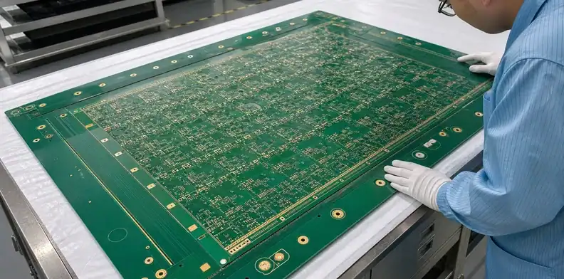
Quick Answer: Large PCB panelization is a production-panel decision, not simply a drawing that repeats the finished board. Confirm working-panel size, process margins, orientation, boards per panel, coupons, rails, tooling, separation method and x-out policy. A few millimeters can change nesting, equipment fit and unit cost, so the fabricator should return the production panel for approval.
Large PCB panelization becomes difficult when the finished outline consumes most of the usable process field. Material utilization falls, rails compete with product area, and one defect can remove an entire panel’s output. Customer assembly arrays and fabricator production panels also serve different purposes and should not be treated as the same object.
This article shows how to review the production panel without taking process ownership away from the fabricator. It focuses on material use, yield exposure, tooling and the approvals that prevent a late quotation change.
Table of Contents
- Separate finished board, customer array and production panel
- Calculate usable material rather than nominal sheet area
- Choose orientation from the full process route
- Allocate rails, coupons and tooling features
- Select separation and edge strategy
- Control x-outs and good-board output
- Connect panel design to assembly
- Approve the panel before tooling release
Separate finished board, customer array and production panel
Decision point: Define which outline is the shipped product, which is customer-controlled and which belongs to the fabricator’s process.
The finished board is the functional PCB after all removable material is gone. A customer array may hold several boards or include rails required for assembly. The fabricator production panel can contain one or more finished boards or arrays plus process borders, coupons and tooling.
Confusing these levels causes dimensional errors and false cost comparisons. A quotation based on a finished outline may change when a customer-controlled rail drawing arrives. Conversely, forcing a complete production-panel drawing can prevent the supplier from using the qualified route.
The Large Format PCB manufacturer page should receive both finished and customer-controlled outlines. Ask the supplier to return the proposed working panel and identify process ownership.
| Object | Typical owner | Approval question |
|---|---|---|
| Finished board | Customer design | Does it meet product geometry? |
| Customer array | Customer with assembler input | Does it meet assembly and separation needs? |
| Production panel | Fabricator | Does it fit every fabrication process? |
| Shipping support | Supplier/customer agreement | Does it protect the delivered condition? |
Calculate usable material rather than nominal sheet area
Bottom line: Utilization should use the processed panel and required margins, not a simple finished-area divided by purchased-sheet-area calculation.
Plating contact, registration targets, coupons, drill entry/backup allowance and routing clearance consume border area. Some materials or copper constructions need larger process margins. Grain direction, foil availability and laminate sheet format can constrain orientation.
The panel example in Altera AN 613 separates the usable area from the nominal panel and allows space between boards for routing. Its dimensions describe that example; obtain the corresponding borders and spacing for the proposed large-board construction.
Illustrative nesting calculation—not a factory quotation: assume a 530 × 530 mm production panel with 15 mm borders, leaving 500 × 500 mm, and a 5 mm routing gap. A 250 × 490 mm board fits once; two need 505 mm. Reducing the 250 mm dimension to 245 mm lets two boards occupy 495 mm. Finished-board area divided by production-panel area changes from 43.6% to 85.5%. Confirm borders, routing gaps, coupons and permitted orientation with the fabricator before changing the outline; a geometric gain does not establish the price saving.
The general PCB panel cost article covers common utilization levers. Large PCB panelization adds equipment fit and single-board yield exposure.
A utilization percentage is useful only when the denominator and required process borders are visible.
Material utilization should be reviewed by construction. A standard FR-4 sheet, a named low-loss laminate and a metal-core panel may have different available formats, margins and grain constraints. A nesting improvement shown on one generic rectangle may not apply to the approved material. Ask the supplier to tie the panel drawing to the signed stack-up or material specification.
Consider repeatability, not only first-order area. A panel with minimal border may look efficient but leave insufficient stiffness or process-control space. If the tighter nest increases handling damage or makes coupons unrepresentative, the apparent saving can reduce good-board output.
Choose orientation from the full process route
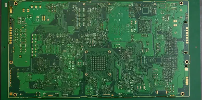
In practice: The best nesting orientation must also satisfy imaging, lamination, plating, drilling, routing, test, grain direction and handling.
Rotating a long board may improve material use but exceed machine width, weaken conveyor support or place critical features near a process edge. Copper distribution and long-axis behavior can affect flatness. The same panel may need different support during wet processing and electrical test.
Ask the fabricator to explain the governing orientation constraint. Record whether the panel rotates between operations and whether tooling features remain valid in both directions. If step imaging or sectional inspection is proposed, include overlap and registration controls in the approval.
Do not optimize a CAM thumbnail without the stack-up and process route. A two-layer long board and a multilayer version may require different panel orientation even with the same finished outline.
Long-axis orientation can also affect assembly. Conveyor support, stencil printing and reflow may prefer a different direction from fabrication nesting. When the customer requires an intact assembly array, choose one orientation that the full route can support or define a controlled transfer between fabrication and assembly formats.
Allocate rails, coupons and tooling features
Evidence check: Every nonproduct feature should have a purpose, owner and removal rule.
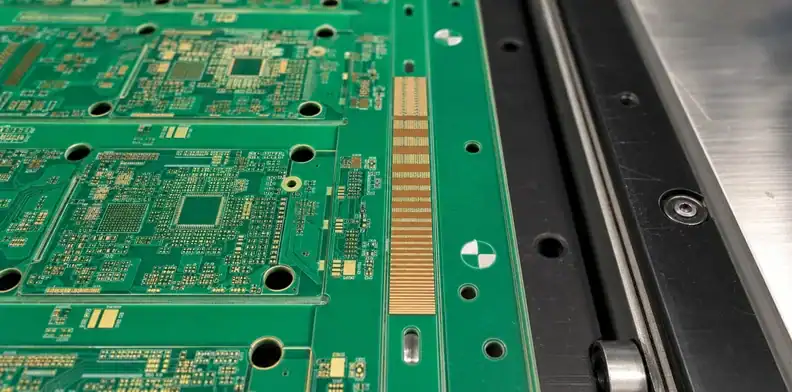
Fabrication borders may carry tooling holes, registration targets, plating contact, impedance coupons, microsection coupons and lot identity. Assembly rails may carry fiducials, tooling holes and conveyor support. The required width and location depend on equipment and the board’s component/edge-clearance design.
Coupons need representative construction and processing. Squeezing them into leftover space without review can make test results less meaningful. Tooling holes and global fiducials should be stable relative to the assembly array, while fabrication targets can remain under supplier control.
Use the PCB panel drawing approval article to record dimensions, rail ownership and revision. Do not let a sales PDF become the only approved panel definition.
| Panel feature | Purpose | Approval owner |
|---|---|---|
| Fabrication border | Process handling and contact | Fabricator |
| Assembly rail | Conveyor and fixture support | Customer/assembler |
| Impedance coupon | Process verification | Customer requirement + fabricator design |
| Breakaway tabs/V-score | Separation | Joint DFM approval |
Preserve the features that prove and handle the process before chasing the last percentage of utilization.
Before stencil or fixture tooling is ordered, send the finished outline, customer rails and assembly constraints for a working-panel review. The returned drawing should separate customer-controlled interfaces from fabricator process features.
Keep supplier-added copper features away from RF, high-voltage and sensitive edge zones. Copper balancing or plating thieves should be reviewed against electrical clearance and removal conditions. Identify which border artwork may change without customer approval and which features—such as a qualification coupon—are controlled by the customer specification.
Select separation and edge strategy
Decision point: Choose routing, tabs, V-score or another method from outline geometry, component clearance, edge quality, stress and delivered format.
V-score suits straight separation lines and compatible thickness/stack-up, but it imposes geometry and residual-thickness constraints. Routed tabs handle irregular outlines but need tab placement, mouse-bite or solid-tab decisions and a controlled removal process. Very long edges can accumulate separation stress or leave unacceptable burrs.
Identify components, copper and connectors close to the edge. Define whether the supplier ships the panel intact, removes rails or delivers individual boards. If depaneling happens after assembly, review component strain and fixture support with the assembler.
Finished-edge requirements such as bevels, plated edges or tight connector interfaces may make a generic breakaway method unsuitable. Put those conditions on the finished-board drawing and verify them against the panel plan.
Simulate separation forces for thin or heavily populated long boards. Support the product near the cut and keep bending away from brittle components or large ceramic packages. For bare boards, inspect residual tabs, burrs and edge delamination before packaging. State whether edge finishing occurs before or after electrical test because the delivered outline can affect fixtures.
Control x-outs and good-board output
Record rule: Purchase orders should define whether defective positions are allowed and how good-board quantity is counted.
On a one-up large panel, one electrical or dimensional reject removes the whole panel output. On a customer array, an x-out may be acceptable to one assembly line and prohibited by another. The quote should state guaranteed good boards, allowed x-outs, marking method, overbuild and replacement policy.
Do not use a percentage yield alone. Track panels started, good boards, rejected positions and dominant defect category. This makes repeat-order improvement possible and prevents a supplier from hiding shortages inside an average.
The PCB x-out panel policy provides a decision framework for accepting or rejecting partial arrays.
Contract for usable boards or accepted arrays, not merely processed panels.
Quantity planning should account for whole panels. If the nest is one-up, every spare board requires another panel start. Define overbuild and maximum extra quantity rather than leaving the supplier to choose. For expensive material, customer approval may be appropriate before starting a replacement panel after a late reject.
Connect panel design to assembly
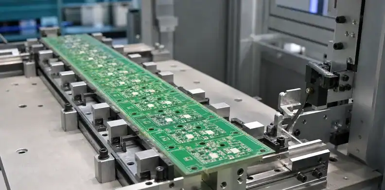
What this means: A fabrication-efficient panel can still fail at solder-paste printing, placement, reflow, AOI or depaneling.
Confirm maximum rail width, panel length, weight, conveyor edge clearance, underside keep-outs and permitted support pins. Long thin boards may need a carrier. If components sit near the edge, rails may need to protect them or provide handling clearance.
Stencil design and printer support should use the approved assembly array. Reflow orientation and support can influence sag, and AOI and test fixtures must cover the same delivered format. Apply the SMT array requirements when preparing that format, then check how it fits the oversized fabrication panel and affects material use.
Review bare-board and assembly panel drawings together. A change made to solve fabrication utilization can invalidate an assembly carrier or stencil.
Confirm traceability after separation. If individual boards leave a customer array, lot and revision marking should remain readable on each board or be linked through controlled packaging. Otherwise a mixed lot can lose the evidence associated with its original production panel.
Approve the panel before tooling release
Freeze the production panel only after customer, fabricator and assembler agree on outlines, ownership, evidence and delivered format.
The approval package should show finished dimensions, array dimensions, production panel, orientation, spacing, borders, tooling, fiducials, coupons, separation, x-out policy and part/revision identity. Mark supplier-controlled features so routine optimization does not require unnecessary customer redrawing.
Reopen approval when the finished outline, stack-up, thickness, copper, separation method or assembly equipment changes. A quantity change can justify a different nesting plan, but it should not silently alter functional rails or coupons.
Archive the approved drawing and supplier disposition with the purchase order. At repeat order, compare the returned panel to the baseline. A supplier may reasonably optimize internal tooling, but any change that affects coupons, customer rails, delivered format, x-out policy or critical support requires the agreed review.
Run a short cross-functional review before approval. Design should verify finished geometry and keep-outs; fabrication should own process borders and nesting; assembly should verify rails, fiducials, support and separation; quality should verify coupons, traceability and acceptance; procurement should verify good-board quantity and tooling ownership. One annotated panel drawing is easier to control than separate assumptions in five email threads.
Do not use panel approval to freeze nonfunctional supplier details forever. Mark a controlled interface around customer requirements, then allow the fabricator to optimize purely internal targets within that interface. This preserves manufacturing flexibility while preventing changes that affect assembly equipment or qualification evidence.
For pilot lots, compare planned and actual material utilization, x-outs and separation quality. If the board is consistently one-up, further outline reduction may have no economic value until the next real nesting threshold. Use production evidence to prioritize redesign effort instead of chasing percentage-area savings.
Panel drawings should use unambiguous units, tolerances and coordinate origins. Identify whether dimensions refer to routed edges, score centerlines or nominal artwork. Show tab and score details at a readable scale and reference the finished-board drawing instead of duplicating critical dimensions with a second value.
Control data handoff as well as the PDF. The CAM package, customer array data, assembly drawing and approved panel drawing must describe the same revision. If the supplier generates the panel, require a returned approval artifact and checksum or revision identifier before stencil, fixture or test tooling is ordered.
A change in order quantity can justify a new nest. Review it as a controlled cost proposal, not an automatic process update. Preserve all functional interfaces and reapprove only the rows that change; this keeps repeat-order review fast without sacrificing traceability.
Record the panel version on stencil, fixture and test-tool orders. That small control prevents downstream tooling from being built against a preliminary rail width or obsolete separation pattern while the PCB data has already moved to a later revision.
The quote, panel drawing and manufacturing data must reference the same revision before tooling begins.

Frequently Asked Questions
How does panel utilization affect a large PCB quote?
It determines how much processed material and capacity produce each good board. Small outline changes can cross nesting thresholds and create stepwise price changes.
Should the customer draw the production panel?
Usually the fabricator should own fabrication borders and nesting. The customer should control finished geometry and any assembly array or rails required by downstream equipment.
Is V-scoring better than tab routing for a long PCB?
Neither is universally better. Use outline geometry, thickness, edge quality, component clearance and separation stress to choose.
Can a large PCB be panelized one-up?
Yes. One-up is common when the outline consumes most of the usable field, but process borders, coupons and tooling still make it a production panel.
What should a panel approval include?
Include all outlines, dimensions, orientation, spacing, rails, tooling, fiducials, coupons, separation, delivered format, x-out policy and revision identity.
Written by the QueenEMS Engineering Team.
Send the finished outline and assembly constraints to identify the best production-panel option before tooling.
Review My Large PCB Panel Plan
Upload your files today · Free DFM check before production · Ship worldwide
Get your PCB prototypes in as fast as 24 hours. We handle FR4, Rogers, and hybrid boards up to 40 layers in volume production, with advanced builds subject to engineering review — free prototypes for 2–4 layer FR-4 boards, no minimum order.
Just upload your Gerber + BOM — we source every part, assemble, and inspect (AOI + X‑Ray) so you don't have to chase suppliers. Boards ship in as fast as 24 hours.