
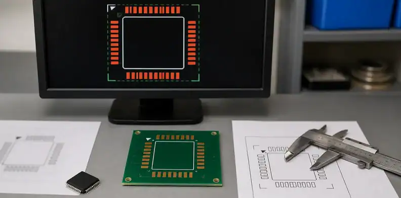
Quick Answer: AI PCB footprint verification starts with the exact manufacturer part number, not a convincing library name. Check land pattern geometry, symbol pins, package suffix, pin 1, polarity, exposed pad, height, and assembly clearance before the quote. The fabricator can review buildability, but the buyer must prove the part placed in CAD is the part being purchased.
AI PCB footprint errors usually survive bare-board fabrication and appear at assembly, where they are more expensive to fix. A pad can be cleanly etched and still be the wrong pad for the package on the BOM. This article focuses on the order-stage checks that should happen before assembly pricing or prototype release.
Table of Contents
- Can you trust an AI-selected footprint?
- What should a two-minute footprint check include?
- How do symbol pins and footprint pads get mismatched?
- Which package names cause the most confusion?
- How do polarity and pin 1 errors show up?
- What can the assembler catch before placement?
- What should you send for assembly quote review?
- How should AVL substitutions be controlled?
- What should the footprint review record say?
Can you trust an AI-selected footprint?
No. Treat the selected land pattern as unverified until it is matched to the exact MPN datasheet and package drawing.
AI tools may choose a generic SOIC, QFN, USB connector, or regulator footprint that looks plausible but misses pitch, body width, exposed pad size, pin count, or suffix. The risk grows when the BOM line contains alternate manufacturers or package codes.
Keep the footprint evidence with the wider AI-generated PCB release checklist when a generated-board order package also needs DRC, Gerber, stackup, and assembly release controls.
For a generated part library, compare the land pattern against the manufacturer’s recommended footprint and not just a community package name. The practical reason is that library names often hide pad-size or exposed-pad differences.
For a generated part library, capture the MPN, datasheet package code, land-pattern source, and reviewer who accepted the pad geometry.
Fit rule: A footprint is not approved until the exact MPN, package drawing, and CAD pads agree.
The practical check is to compare the land pattern against the exact ordering code, not only against a package family. A QFN, SOT, connector, or module can share a familiar body name while changing exposed-pad size, lead pullback, pin count, mounting peg, or shield outline. When the datasheet offers several recommended patterns, record which option was chosen and why it fits the assembly process.
What should a two-minute footprint check include?
Check pitch, pad size, pad numbering, pin 1, polarity, exposed pad, courtyard, and component height. The PCB DRC vs DFM limits page helps separate package proof from general rule-deck clearance checks.
Print or view the footprint at 1:1 scale when the part is mechanical, connector-heavy, or fine pitch. Compare the assembly layer against the datasheet’s recommended land pattern, not only against a library description.
For a fast prototype with connectors, print or view the connector region at 1:1 scale and check shell tabs, pegs, keying, and board edge position. The practical reason is that connectors can pass electrical checks while failing mechanical fit.
For connector-heavy prototypes, mark the mating-side orientation, mounting peg holes, shell keepout, and board-edge relationship on the assembly review.
Footprint verification map:
| Check | Evidence | Failure avoided |
|---|---|---|
| Pitch and pad | Datasheet land pattern | Unsolderable part |
| Pin map | Symbol-footprint comparison | Wrong connection |
| Polarity | CPL plus assembly drawing | Rotated component |
| Height | Mechanical drawing | Enclosure clash |
How do symbol pins and footprint pads get mismatched?
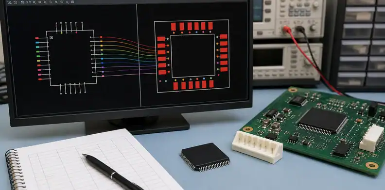
A symbol can be electrically legal while the footprint maps pins to the wrong pads.
AI part generators and copied libraries can swap gate pins, connector positions, thermal pad naming, or package variants. The schematic may simulate or compile, but the assembled board can connect the wrong physical lead.
For a symbol created from a datasheet table, trace every numbered pin from schematic symbol to footprint pad and BOM MPN. The practical reason is that pin names can be logical while physical numbering is wrong.
If a symbol-to-pad mismatch is found, revise the library item and regenerate BOM, CPL, and assembly drawing from the same source.
Mapping check: Pin numbers in the symbol, footprint, datasheet, and BOM must describe the same physical terminals.
Pin mapping should be reviewed as a table, not only as a rendered schematic symbol. Look for swapped differential pairs, duplicated power pins, hidden no-connect pins, thermal pads that need stitching vias, and configurable pins that changed function in firmware. A short CSV export or annotated screenshot can save the assembler from discovering the mismatch after stencil, placement data, and first-article inspection are already prepared.
Which package names cause the most confusion?
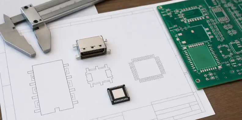
Family names such as QFN, DFN, SOIC, SOT-23, and USB connector are not enough.
Package suffixes define body size, pitch, lead count, exposed pad, height, and sometimes pin order. Connector series can share a marketing name while changing shield tabs or locator pegs.
For a package family with suffix variants, read the body size, pitch, height, and thermal-pad dimensions from the exact suffix. The practical reason is that generic QFN or SOT labels do not define the assembled part.
When suffix variants change body size or exposed-pad dimensions, freeze the approved MPN list before purchasing substitutes parts.
How do polarity and pin 1 errors show up?
They often show up as perfectly assembled boards that do not power up or communicate.
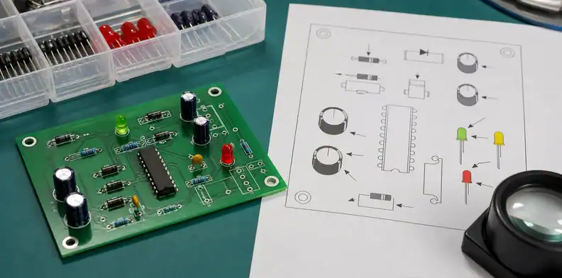
Check diode cathodes, electrolytic capacitors, LEDs, IC pin 1 marks, connectors, switch orientation, and polarized mechanical parts. Silkscreen alone is not reliable; assembly needs CAD polarity, CPL rotation, and BOM identity to agree.
For a polarized assembly, verify that CAD polarity, CPL rotation, silkscreen, and datasheet markings all point the same way. The practical reason is that one inconsistent source can rotate a part during placement.
For polarized assembly, check the silkscreen mark, centroid rotation, datasheet pin 1, and assembly drawing before stencil work starts.
AI footprint risk by part type:
| Part type | Common AI miss | Manual check |
|---|---|---|
| QFN/DFN | Exposed pad size | Thermal pad drawing |
| Connector | Peg and shield geometry | Series drawing |
| Regulator | Package suffix | Exact MPN |
| LED/diode | Polarity mark | Assembly layer |
Orientation rule: Polarity must be visible in CAD data and assembly files, not only remembered by the designer.
Polarity should be checked in three places: the schematic symbol, the PCB silkscreen or assembly drawing, and the centroid rotation used by the pick-and-place program. Diodes, LEDs, electrolytic capacitors, connectors, IC pin 1 marks, and shielded modules all fail in different ways. The quote package should make the intended orientation visible before the assembler builds the feeder setup.
What can the assembler catch before placement?
The assembler can question mismatched BOM/CPL data, impossible rotations, or obvious package conflicts.
Assembly review cannot guarantee that the circuit designer chose the correct footprint for the application. It also cannot know whether an AI symbol’s logical pin names match the firmware or cable harness.
For a DFA review, ask the assembler to report conflicts between BOM, CPL, pads, and assembly drawing. The practical reason is that the assembler can catch mismatch evidence but cannot invent the designer’s intent.
For DFA review, record the exact placement obstacle, component height issue, polarity risk, or courtyard conflict that must be resolved.
What should you send for assembly quote review?
Send Gerber or ODB++, BOM, CPL, assembly drawing, polarity notes, datasheets for critical parts, and known substitutes. Use AI PCB Gerber review before quote when the land-pattern decision has to be checked against exported fabrication data.
For parts with alternate MPNs, state whether substitutions are allowed and whether the same footprint is confirmed. Keep that confirmation in the release record when the footprint review is part of a wider generated-board order.
For an assembly quote request, send datasheets for critical, unusual, or alternate parts with the BOM and CPL. The practical reason is that pricing based on an unverified library can hide rework or part-change cost.
Close an assembly quote request by matching BOM, CPL, datasheets, polarity notes, and substitution rules to the same revision.
RFQ signal: Assembly quote files should prove part identity before price and lead time are compared.
How should AVL substitutions be controlled?
Control substitutions by footprint, electrical role, package code, and assembly evidence, not by price alone.
If purchasing may use alternates, each alternate MPN should be checked against the same land pattern and rotation requirement. A substitute that is electrically similar can still use a different exposed pad, height, polarity mark, or thermal tab. Keep approved alternates in the BOM or AVL so the assembler does not choose a part that fits the description but not the pads.
Alternate parts need footprint approval, not just electrical approval. A substitute regulator, connector, crystal, or sensor may match the BOM value while changing pad width, height, coplanarity, lead finish, keepout, or thermal pad recommendation. If alternates are allowed, list which MPNs share the released footprint and which ones require a separate land-pattern review before purchasing uses them.
The safest AVL note separates three decisions. First, state whether the substitute is electrically acceptable. Second, state whether it fits the released land pattern and assembly height. Third, state whether purchasing may use it without another engineering review. Many assembly delays happen because only the first decision is recorded. A part can meet voltage, current, and tolerance requirements while needing a different pad, thermal relief, or polarity mark. That is why the substitution record should name the exact MPN, the released footprint, and the assembly evidence used for approval.
What should the footprint review record say?
The record should name the datasheet revision, footprint source, reviewer, and any approved assembly exceptions.
For connectors, ICs, LEDs, polarized capacitors, and mechanical parts, include the exact drawing or datasheet page used for the decision. If the assembler raises a question, record whether the answer changes BOM, CPL, assembly drawing, or the PCB footprint itself. That record becomes useful when the same AI design is revised later.
Record rule: Footprint approval should be traceable to a part drawing, not to a library name.
A practical footprint review also protects the purchasing conversation. When a buyer asks for a fast assembly quote, the supplier may price the build from the BOM and CPL before anyone notices that the land pattern came from a generic library. Add a short note beside every critical component that says footprint checked against datasheet, alternate package not allowed, or alternate package approved on same land pattern. Those notes keep the quote from turning into a silent AVL substitution.
The readback is just as useful as the first check. Before PO release, compare the final BOM line, CAD reference designator, CPL rotation, and assembly drawing for the parts most likely to fail: connectors, LEDs, polarized capacitors, QFN/DFN packages, BGAs, switches, and any part with a thermal pad. If one source disagrees, stop the assembly quote until the owner fixes the source file rather than answering in chat. This small pause is cheaper than discovering the mismatch after stencil, placement, or reflow planning has already started.
For assembly quote review, send QueenEMS the BOM, CPL, assembly drawing, Gerbers, critical datasheets, approved substitutes, and polarity questions through the QueenEMS contact page. Identify the revision, build quantity, footprint exceptions, and any MPN that still needs approval.
A strong footprint record names the MPN, package drawing revision, land-pattern source, reviewer, date, and any assembly condition such as hand soldering, reflow-only, paste aperture reduction, or selective solder clearance. That record does not need to be long, but it should be specific enough that a later buyer can see why the released pads match the ordered part.
For AI-assisted library work, add the reason the footprint was considered risky. Examples include generated library, copied symbol, connector series ambiguity, thermal-pad package, alternate supplier, or polarity-sensitive part. That short reason helps a later reviewer decide whether the same check must be repeated after revision. If the risk has been closed, keep the evidence with the released files rather than leaving the answer in a message thread. The goal is not more paperwork; it is a record that prevents the same footprint question from returning at every quote, stencil, and first-article step.
FAQ
Can a factory fix a wrong footprint?
Usually no. The factory can flag obvious assembly conflicts, but the buyer must approve the correct land pattern from the datasheet.
Is a 1:1 print still useful for AI PCB footprints?
Yes. A 1:1 print catches scale, connector fit, and orientation problems that are easy to miss on screen.
What files prove footprint intent?
The BOM, CPL, assembly drawing, datasheet land pattern, and CAD footprint should all identify the same part and orientation.
Can I approve an AI footprint if the package family matches?
No, package family alone is not enough because lead pitch, body size, pad geometry, pin 1 orientation, and assembly courtyard can still differ. Approve the footprint only after the land pattern, datasheet package code, and assembly drawing all describe the same part.
Sources
Written by the QueenEMS Engineering Team
Upload your files today · Free DFM check before production · Ship worldwide
Get your PCB prototypes in as fast as 24 hours. We handle FR4, Rogers, and hybrid boards up to 40 layers in volume production, with advanced builds subject to engineering review — free prototypes for 2–4 layer FR-4 boards, no minimum order.
Just upload your Gerber + BOM — we source every part, assemble, and inspect (AOI + X‑Ray) so you don't have to chase suppliers. Boards ship in as fast as 24 hours.