

Quick Answer: In sourcing searches, “single-sided pcb” means a board with one conductive copper layer. It is a strong option for low-density circuits that can route cleanly without a dedicated second copper layer. Choose a double-sided board when routing congestion, ground return, EMI control, thermal spreading, board area, or assembly access makes one layer awkward or unreliable. Compare both versions at the same outline, material, copper, finish, test scope, and quantity before assuming the one-layer board costs less.
A one-layer circuit can be the most disciplined answer to a simple electrical problem. It can also become a false economy when the layout grows, jumpers multiply, or a large outline is needed to avoid trace crossings. The layer decision belongs early in schematic and mechanical development because it affects routing, grounding, fabrication, assembly, test access, and enclosure fit.
Search results often describe a single-sided PCB as “components on one side.” That shortcut is incomplete. The defining feature is one conductive copper layer. Component placement and soldering method are separate assembly choices, and confusing them can produce the wrong quotation or DFM assumption.
Table of Contents
- What makes a PCB single-sided
- Where one copper layer works well
- Routing limits appear before fabrication
- Ground return and EMI can force a second layer
- Thermal and current demands change the answer
- Assembly method affects the board choice
- Single-sided fabrication removes some steps
- Cost depends on more than layer count
- Prototype evidence should decide the release
- Choose one or two layers in the RFQ
What makes a PCB single-sided
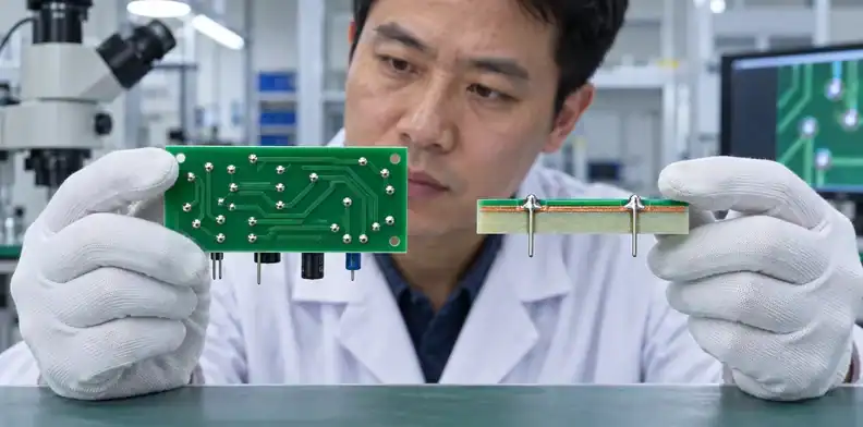
The search phrase “single-sided pcb” describes a board with one patterned conductive copper layer on an insulating substrate. Solder mask protects much of that copper, surface finish protects exposed pads, and legend can identify components or test points.
Copper layers and component sides are different
“Single-sided” describes the circuit construction, not a universal placement rule. In a conventional through-hole board, component bodies often sit on the non-copper side while leads pass through unplated or plated holes and are soldered on the copper side. A surface-mount design can place components directly on the copper side. Mixed arrangements are possible if clearances, process access, and assembly sequence support them.
| Term | What it actually describes | What it does not guarantee |
|---|---|---|
| Single-sided PCB | One conductive copper layer | Only one component side |
| Double-sided PCB | Copper patterns on both faces | Components must occupy both faces |
| Through-hole assembly | Leads pass through drilled holes | A multilayer board |
| Surface-mount assembly | Parts solder to surface pads | Two conductive layers |
The construction can use FR-4, paper-based laminate, metal-backed material, a flexible film, or another qualified substrate. Those choices change thermal, mechanical, electrical, flammability, and fabrication behavior. Layer count by itself is not a material specification.
IPC-6012 is the IPC performance specification for rigid boards, and its scope includes one-layer, two-layer, and multilayer constructions. Your drawing still needs to state the applicable revision, performance class or acceptance basis, and product-specific requirements.
Where one copper layer works well
One layer works best when the circuit is sparse, low enough in speed, mechanically generous, and easy to route without compromising return paths or test access. Typical candidates include indicator boards, simple controls, relays, low-complexity power interfaces, appliance subassemblies, LED products, and educational or serviceable equipment.
The application name is not proof. An LED board may be electrically simple but thermally demanding. A relay board may switch high voltage and need wide creepage distances. A low-speed sensor may operate beside a motor and face noise. Evaluate the actual circuit and enclosure rather than copying a familiar product category.
| One-layer fit signal | Why it supports the choice | Evidence to check |
|---|---|---|
| Low connection density | Traces can route without crossings or excessive detours | Completed layout and DRC report |
| Modest signal speed | Return paths and trace length are less demanding | Interface rise time and layout review |
| Stable mechanical area | The board does not need to shrink to fit | Enclosure drawing and keep-outs |
| Simple power distribution | Copper width and temperature rise are manageable | Current map and copper calculation |
| High service visibility | Conductors remain accessible for inspection or repair | Test-point and maintenance plan |
One layer can also support high-volume production, but volume does not make a weak layout acceptable. The design must first fit the electrical and mechanical task. Only then should the sourcing team evaluate whether the simpler process produces a repeatable commercial benefit.
If the product is still at concept stage, the PCB prototype ordering process can separate a layout experiment from a released production build. Prototype quantities should use the same critical outline, connector pattern, material family, and assembly method when those features drive the layer decision.

Routing limits appear before fabrication
A one-layer layout fails as a concept when the required nets cannot route with safe geometry inside the allowed outline. The board may still be drawable, but long detours, necked traces, dense jumper wires, or poor connector placement can create more risk than a second copper layer.
Jumpers are a design signal, not a defect
A small number of planned jumpers can be entirely reasonable. They may preserve a proven single-sided architecture while crossing unavoidable nets. The problem begins when jumpers become the default solution for congestion or when their placement interferes with assembly, inspection, or enclosure clearance.
Track jumper count, type, length, current, insulation, placement side, and assembly method. A zero-ohm surface-mount link, an insulated wire jumper, and a formed component lead do not have the same process or inspection needs. Put intentional jumpers in the BOM and assembly drawing rather than leaving production to infer them from copper gaps.
Connector pin order often determines whether one layer remains practical. Rotating a header, swapping equivalent pins in the schematic, or moving a connector before mechanical release can remove crossings at almost no manufacturing cost. The same change becomes expensive after a molded enclosure, cable, or mating board is frozen.
Use the completed board outline and actual design rules for comparison. The PCB fabrication tolerance review helps distinguish a genuine routing need from an unnecessarily tight rule that raises cost without improving function.

Ground return and EMI can force a second layer
A second copper layer becomes valuable when the circuit needs a continuous return path, controlled loop area, shielding behavior, or cleaner separation between noisy and sensitive nets. Frequency alone does not decide this; edge rate, current loop, cable length, source impedance, enclosure, and emissions requirement all matter.
Return-path evidence to review
On a single copper layer, signal and return conductors share the same routing plane. Every cut, detour, connector transition, and jumper can enlarge a loop. The result may be acceptable for a slow, tolerant circuit, but it becomes risky near switch-mode power stages, clocks, sensitive analog inputs, long cables, radios, or compliance limits.
Review the current path rather than coloring one net “GND” and assuming it behaves as a plane. Identify where source current leaves, where it returns, what conductor carries it, and which noisy loads share that path. A two-layer board can dedicate more continuous copper to reference and power distribution, but it still needs deliberate placement and routing.
| Observation | One-layer response | When two layers are safer |
|---|---|---|
| Few slow digital nets | Route signal and return close together | Return detours around connectors or cutouts |
| Switching current loop | Keep the loop compact and local | Required geometry cannot fit on one face |
| Sensitive analog input | Separate it from load current | Shared return creates measurable noise |
| Cable leaves the board | Define return and protection at the connector | Emissions or immunity margin is uncertain |
| Ground coverage is fragmented | Rework placement and routing | Copper islands remain after layout closure |
The controlled-impedance specification guide is relevant when the electrical interface requires a defined transmission structure. A single-sided article should not imply that ordinary low-speed designs need impedance control, but it should recognize when the electrical requirement has already moved beyond a one-layer answer.

Thermal and current demands change the answer
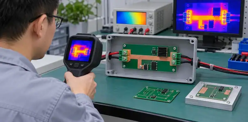
Copper width, thickness, temperature rise, heat sources, airflow, and substrate choice can outweigh the layer-count saving. A one-layer board may provide a wide uninterrupted conductor, while a compact design may need copper on two faces, thermal vias, or a metal-backed construction.
Choose the thermal path before the layer count
Do not use copper weight as a shortcut for the whole thermal design. Thicker copper can reduce conductor resistance, but component junction temperature also depends on pad geometry, copper spreading area, dielectric path, enclosure, ambient temperature, airflow, duty cycle, and neighboring heat sources. The heavy-copper design discussion belongs only when the calculated current or thermal requirement supports it.
Wide available board area can preserve the one-layer option by giving power conductors and clearances more room. A tight enclosure removes that freedom and may justify two copper faces or another substrate. Concentrated LED heat should trigger a verified thermal path and a comparison with an FR-4 versus metal-core LED PCB. High terminal current requires checks at neck-downs, holes, and connectors, while a large temperature gradient calls for a combined layout, material, mounting, and enclosure review.
An illustrative decision shows why the geometry matters. Suppose a one-layer motor-control board routes the power path only by circling the board edge. The trace meets minimum width, but the route is long and passes beside a sensor input. Before claiming a cheaper build, compare a two-layer revision with a shorter power loop and a continuous reference area. Verify both with current loading, temperature measurement at the intended enclosure condition, and noise testing at the sensor. The expected result is conditional: the two-layer option is justified only if the measured electrical or thermal margin improves enough to offset its process cost.
This is an illustrative scenario, not a claimed QueenEMS customer case. Its lesson is to test the actual trade-off rather than assigning reliability to a layer count.
Assembly method affects the board choice
Assembly can preserve or erase the simplicity of a single-sided board. Component technology, placement side, soldering process, support, test access, and rework must match the conductive-layer construction.
Through-hole and SMT are not layer counts
A traditional single-sided through-hole board often places component bodies on one face and solders leads on the copper face. This provides clear visual access but may require wave or selective soldering, lead trimming, and mechanical support for large parts. A surface-mount single-sided board can place parts on the copper face and use reflow, reducing drilled leads while concentrating routing and land patterns in the same area.
Mixed technology may need two thermal processes or selective soldering. Large connectors, transformers, relays, switches, and terminals can impose mechanical loads that copper pads alone should not carry. The assembly drawing should define orientation, staking or hardware where required, and access for solder inspection.
If parts are proposed on both faces of a board with one copper layer, review how each part reaches the copper, how it is soldered, and whether the sequence is repeatable. Do not let “one-layer” become a purchasing label that hides a complicated manual process.
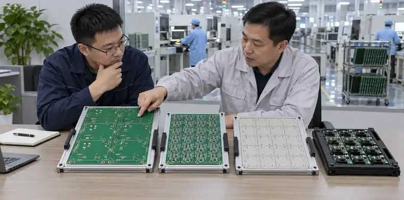
The PCB panelization for assembly can matter even for a simple board. Small, irregular, or edge-sensitive products may need rails, fiducials, tooling holes, or an array that adds cost independently of copper-layer count.

Single-sided fabrication removes some steps
A one-layer rigid board avoids inner-layer processing, multilayer lay-up, lamination registration, and plated interlayer connections when the design does not require plated holes. It still needs controlled imaging, etching, mask, finish, profile, inspection, and electrical test.
| Route stage | Single-sided board | Double-sided plated-through board |
|---|---|---|
| Copper pattern | One external face | Both external faces |
| Interlayer connection | Not applicable | Drilled and plated through holes/vias |
| Lamination | No multilayer lay-up | Usually one base laminate, no multilayer lay-up |
| Registration burden | Copper to holes and outline | Top to bottom copper, holes, and outline |
| Test basis | One-layer netlist | Two-layer netlist and plated connections |
Some low-cost single-sided constructions use non-plated component holes. Others may include plated holes or special terminals. Do not assume the cheapest route from the layer name. State whether holes are plated, whether the board has edge contacts, which surface finish is needed, and how the assembly will be soldered.
The shorter route can reduce opportunities for certain multilayer defects, but it does not guarantee quality. Etch control, mask registration, pad adhesion, hole position, profile tolerance, finish condition, solderability, and packaging still determine whether the board assembles correctly.
Use the PCB manufacturer capability check to verify the actual material and process combination. A factory that can build advanced multilayers may still route simple paper-based, metal-backed, or unusual one-layer constructions through a different qualified line.

Cost depends on more than layer count
Layer count changes process cost, but board area, material utilization, drilling, finish, panelization, test, assembly, and quantity decide the final comparison. A larger one-layer layout can consume more panel area than a compact two-layer design and eliminate the expected saving.
Board area can erase the expected saving
Compare the same electrical function and enclosure constraint. If the one-layer version needs a larger outline, more jumpers, longer assembly time, or manual wiring, include those costs. If the two-layer version needs plated holes and tighter registration but reduces area and assembly steps, include that benefit.
Prototype pricing can also mislead. At very low quantities, setup, shipping, and minimum charges may dominate. At production quantities, panel utilization, test method, assembly cycle, and defect containment matter more. Ask for quantity breaks using the same revision and delivery terms.
Do not accept a universal statement such as “single-sided costs half as much.” The percentage changes with technology and supplier route, and it says nothing about total product cost. A useful quote identifies the assumptions: outline, material, copper, hole count, finish, panel format, test, assembly, quantity, and packaging.
A DFM review before purchase order should close the layer decision before tooling or production material is committed. If the supplier proposes a second layer, require the specific constraint and the revised quote rather than a generic preference.
Prototype evidence should decide the release
The prototype should test the reason for choosing one layer, not merely prove that the circuit turns on once. Verify electrical function, return-path behavior, thermal margin, mechanical fit, assembly repeatability, test access, and service conditions that could expose the choice.
| Decision risk | Prototype evidence | Release condition |
|---|---|---|
| Congested routing | DRC closure and visual review of neck-downs/jumpers | No undocumented workaround |
| Noise or EMI | Measurement in the intended cable and enclosure state | Margin meets the product requirement |
| Current and heat | Loaded temperature and voltage-drop results | Worst-case condition is accepted |
| Assembly access | Pilot build and inspection record | Solder joints and polarity are inspectable |
| Mechanical fit | First-article dimensions and enclosure trial | Connectors, holes, and outline fit |
Record the test configuration. A bare board on a bench may behave differently after long cables, a plastic enclosure, a metal chassis, a nearby motor, or a sealed thermal condition is introduced. The release evidence should reproduce the risk-driving operating state.
If the prototype fails, avoid treating the second layer as the only repair. Connector pin mapping, component placement, grounding, trace geometry, filtering, substrate, enclosure, or assembly method may be the root issue. Fix the mechanism and then decide the construction.
For repeat orders, freeze the accepted netlist, stack-up, material rule, panel, and assembly process. A later component substitution with different pinout, current, package, or switching behavior can reopen the layer decision even if the bare-board outline remains unchanged.

Choose one or two layers in the RFQ
A useful RFQ lets the supplier compare one-layer and two-layer options without changing hidden assumptions. Submit the same outline, schematic intent, Gerber or ODB++ data, material requirement, copper, finish, tolerances, acceptance basis, assembly scope, and quantity breaks.
State whether the supplier may propose an alternate layer count. If yes, ask for the engineering reason, affected files, cost difference, lead-time difference, and any change to assembly or test. The proposal should not silently replace the released design.
The final package should include the items below.
- Controlled fabrication and assembly data with one revision.
- Board outline, mounting, connector, height, and keep-out constraints.
- Maximum current, switching interfaces, sensitive signals, and required test points.
- Substrate and copper requirements, or an explicit equivalency boundary.
- Finish, solder-mask, legend, hole, profile, and panel requirements.
- Prototype verification plan and production quantity breaks.
For a construction comparison, send QueenEMS both layout options, the enclosure drawing, current and interface notes, intended assembly process, prototype quantity, and production forecast. The engineering response can identify the constraint that favors one or two layers, list any DFM changes, and quote both builds on matched assumptions when both are viable.

FAQ
Is a single-sided PCB the same as a one-layer PCB?
Yes. Both terms normally mean that the board has one patterned conductive copper layer.
Can a single-sided PCB use surface-mount components?
Yes. Surface-mount components can be placed on the copper side when the land pattern, routing, soldering process, and inspection access support it.
Can components appear on both sides of a single-sided PCB?
Yes, in some constructions, because component side and copper-layer count are different concepts. The assembly method and electrical connection to the one copper layer must be defined.
Is a single-sided PCB always cheaper?
No. A larger outline, added jumpers, manual assembly, special material, difficult panelization, or low quantity can outweigh the simpler fabrication route.
When should I switch to a double-sided PCB?
Switch when one layer cannot provide clean routing, acceptable return paths, thermal/current margin, mechanical fit, assembly access, or a reliable production process within the product requirements.
Sources
Written by the QueenEMS Engineering Team
Upload your files today · Free DFM check before production · Ship worldwide
Get your PCB prototypes in as fast as 24 hours. We handle FR4, Rogers, and hybrid boards up to 40 layers in volume production, with advanced builds subject to engineering review — free prototypes for 2–4 layer FR-4 boards, no minimum order.
Just upload your Gerber + BOM — we source every part, assemble, and inspect (AOI + X‑Ray) so you don't have to chase suppliers. Boards ship in as fast as 24 hours.