

BT PCB Manufacturer for IC Substrate & Package Applications
Custom BT resin PCB fabrication for BGA, CSP, MEMS, RF modules and Chip LED applications, with engineering review, fine-line control and full batch traceability.
BT Resin Material Support
Fine-Line & Microvia Control
Engineering DFM Review
Fast Quotation & Order Tracking
Why BT PCB Projects Fail at Ordinary PCB Factories
IC substrate PCB manufacturing demands controls that commodity PCB shops rarely have. These are the failure modes we see repeatedly — and the process controls we run to keep them out of your builds.
Ultra-thin core warpage after lamination and reflow
Substrates twist during pressing and bake cycles, breaking BGA joints and forcing costly rework at your downstream assembly line.
Low-CTE material + copper balance + panel-level warpage inspection
Locked-in low-CTE laminate, symmetric copper distribution, and post-lamination warpage measurement on every panel keep flatness within your acceptance spec.
Fine line/space over-etching, residual copper or shorts
Trace geometry drifts beyond IPC tolerance, causing open circuits and shorts that only surface at electrical test — too late in the cycle to fix cheaply.
Exposure compensation + etch control + in-line AOI & line-width measurement
Pre-compensated Gerber, tightly controlled etchant chemistry, and 100% AOI with automated line-width sampling catch geometry drift on the same shift.
Laser microvia misregistration, thin copper or unstable reliability
Weak or misplaced microvias survive electrical test but fail thermal cycling in the field — the worst kind of defect to discover after shipment.
Microvia DFM review + drill compensation + copper plating & microsection
Every stack-up passes microvia DFM, drill positions compensated for material shrinkage, plating uniformity verified by cross-section on every lot.
Batch-to-batch inconsistency in thickness, finish or size
New spins don't match the golden lot, forcing your line to re-tune for every delivery and eating into planned volume ramp.
Fixed material system + lot traceability + first-article confirmation
Locked BOM (brand, model, thickness), lot-level material records, and first-article approval before mass release keep repeat orders identical.
Sales staff can't answer packaging or substrate questions
Days lost waiting for engineering feedback, imprecise DFM reviews, and no clear owner for technical decisions.
Substrate engineers join every quote and DFM review directly
Direct engineering contact from quote through delivery — no sales middleman relaying half-answers, so decisions happen in hours instead of days.
Send your Gerber and package spec — our engineers will flag the risks specific to your design.
Request Engineering FeedbackWhat Is a BT PCB and Why Is It Used in IC Packaging?
A BT PCB (Bismaleimide-Triazine resin substrate) sits between your silicon die and the motherboard — translating fine-pitch chip I/O into board-level pitch while adding mechanical support and thermal stability.
Chip / Die
Silicon die with fine-pitch I/O pads (down to 40μm)
BT Package Substrate
BT resin PCB redistributing die signals to board pitch
Motherboard PCB
Standard FR-4 board where the package mounts
Signal Redistribution
Redistribute the die's fine-pitch I/O (down to 40μm) to solderable BGA / CSP pitches that a standard motherboard PCB can actually accept — enabling advanced silicon to reach mainstream assembly lines without exotic PCB tech.
Mechanical & Electrical Support
Provide a rigid platform for wire-bond or flip-chip attach, with low-loss copper routing that preserves signal integrity — protecting your silicon investment from mechanical stress and signal degradation over the product's field life.
Thermal & Dimensional Stability
Deliver a low-CTE base (3–8 ppm/°C) that matches silicon expansion and dissipates heat outward — extending package field life and cutting warranty return rates on high-power and thermally-cycled devices.
Need help deciding whether your package should sit on BT substrate?
Talk to a Substrate EngineerBT PCB vs. FR-4 vs. ABF Substrate
Typical positioning for each substrate family — use as guidance for early material screening. Final selection always depends on your specific package pitch, I/O count, layer requirements and reliability targets.
| Comparison Item | FR-4 PCB | BT Substrate | ABF Substrate |
|---|---|---|---|
| Common Positioning | General-purpose PCB, control boards | BGA, CSP, MEMS, memory, RF, LED packaging | High-I/O, high-performance processor packaging |
| Line Density | Standard | Fine to high-density | Ultra-high density |
| Dimensional Stability | Standard | Higher (low-CTE resin) | High |
| Cost Level | Lower | Mid-to-high | Higher |
| Best-fit Customer | General electronic products | Mid-to-high density IC packaging | Complex CPU / GPU / accelerator packaging |
Not sure whether your design requires BT or ABF? Send us the package type and minimum line/space — we'll recommend the right substrate family for your build.
Get Material RecommendationBT PCB Solutions by Package Type and Application
Select an application to see the recommended BT laminate, typical structure and the manufacturing focus points that drive yield for that package family.
BGA / PBGA Substrate PCB
Reliable BGA and PBGA package substrates built on high-Tg BT laminate with symmetric copper distribution — engineered for the thermal cycles your BGA products actually see in service.
CSP / FC-CSP Substrate PCB
Chip-scale and flip-chip CSP substrates on low-CTE BT — matched to silicon-die expansion so underfill and solder joints survive JEDEC thermal cycling with margin.
MEMS and Sensor Substrate PCB
Halogen-free BT substrates on thin-core CCL — engineered for the dimensional precision that MEMS calibration depends on through soldering and end-of-life thermal cycles.
Memory IC Substrate PCB
High-speed BT substrates for DDR, LPDDR and NAND flash packages — low-Df laminate protecting the eye-diagram margin your memory validation depends on.
RF Module and Communication Substrate PCB
Low-loss BT substrates for 5G, WiFi and mmWave modules — stable Dk into the microwave range so your RF S-parameters land where the simulation says they will.
Chip LED and Automotive Module Substrate PCB
High-Tg BT substrates with high thermal aging resistance — surviving under-hood 125°C operation and LED junction temperatures well past standard-laminate limits.
Building a package we haven't listed? We ship BT substrates for medical, aerospace and IoT applications too.
Discuss Your ApplicationBT PCB Manufacturing Capabilities
Verified process parameters from our engineering team — real production capabilities on live orders, not marketing brochure numbers. Cross-check these against your design tolerances before finalizing the stack-up.
| Parameter | Typical Production | Advanced Capability |
|---|---|---|
| Layer Count | 2 – 8 layers | Up to 16 layers (sequential build-up) |
| Board Thickness | 0.20 – 0.80 mm | 0.10 mm min / 1.20 mm max |
| Minimum Line / Space | 40 / 40 μm | 25 / 25 μm (mSAP process) |
| Minimum Laser Microvia | 75 μm | 50 μm (aspect ratio up to 1:1) |
| Minimum Pad Pitch | 0.40 mm BGA | 0.30 mm CSP |
| Layer Registration Tolerance | ±50 μm | ±25 μm |
| Copper Thickness | 18 – 35 μm (0.5 – 1 oz) | 12 μm to 210 μm (up to 6 oz) |
| Surface Finish | ENIG, ENEPIG | Soft Gold, Hard Gold, Immersion Silver |
| Warpage Tolerance | ≤ 0.75% | ≤ 0.50% (per IPC-6012) |
| Impedance Control | ±5% | ±5% (matched-pair differential) |
| Panel / Array Size | Up to 250 × 340 mm | Up to 300 × 400 mm |
| Prototype Quantity | 5 – 50 panels | From 1 panel (fast-track) |
| Mass-Production Volume | 500 – 5,000 panels / month | Up to 20,000 panels / month |
Note: Advanced capability parameters are demonstrated on qualified stack-ups and may require additional lead time or engineering review. Send your design to confirm the exact tolerances we can hold for your specific build.
Need parameters beyond this table? Our engineers can confirm feasibility for custom designs.
Download Full Capability Data SheetBT PCB Manufacturing Process — From DFM to Final Inspection
Eleven controlled steps from Gerber review to final packaging, each gated by inspection so problems get caught inside the factory instead of arriving on your assembly line.
Gerber, Stack-up & Package Review DFM Gate
Substrate engineer audits Gerber files, proposed stack-up and target package parameters against manufacturability limits — catching design conflicts before tooling starts.
BT Material Verification & IQC Inspection
Incoming inspection of BT laminate, prepreg and copper foil against CoC and internal spec — every lot logged with mill certificate and internal batch ID.
Inner-Layer Imaging & Fine-Line Patterning
LDI or high-resolution photo-imaging with pre-compensated Gerber for etchant undercut — holds trace geometry within IPC Class 3 for 25/25μm designs.
Lamination & Shrinkage Compensation
Vacuum-press lamination with material-specific pressure and temperature curves; X-Y shrinkage compensated in tooling data to keep layer-to-layer registration on target.
Laser Drilling & Microvia Formation
UV or CO₂ laser drilling for blind and buried microvias down to 50μm, with drill position compensated for measured panel shrinkage.
Electroless & Electroplating
Desmear, electroless copper seed and pulse-plating fill for blind and through vias — plating uniformity verified per panel to prevent voids and weak barrels.
Pattern Etching
Fine-line etch with controlled etchant chemistry and in-line line-width sampling — catches geometry drift on the same shift instead of at final AOI.
Solder Mask Application
LDI mask exposure for fine mask openings and controlled cure profile — delivers uniform mask height for consistent wire-bond and flip-chip attach downstream.
Surface Finish Plating
ENIG, ENEPIG, soft gold, hard gold or immersion silver — plating thickness verified against bond-pull and solder-joint reliability targets.
AOI, E-Test, Dimensional & Warpage QC 100% Inspection
Automated optical inspection, flying-probe electrical test, panel dimensional check and warpage measurement — every panel individually verified before final packaging.
Packaging & Lot Traceability Shipment
Vacuum-sealed with moisture-barrier bag and desiccant, labeled with internal lot ID that ties back to raw-material batch — full traceability preserved from mill to your dock.
Want to walk through this process with a specific stack-up or package in mind?
Schedule a Process ConsultationBT PCB Materials and Stack-Up Options
Qualified BT laminates, prepreg systems, stack-up structures and surface finishes we hold in stock. Every material has a manufacturer data sheet on file and lot-level traceability — nothing gets substituted without your written approval.
BT Material Options
Low-CTE BT Laminate
Silicon-matched thermal expansion prevents underfill cracking in flip-chip designs — protecting your die-to-substrate bond through JEDEC MSL-3 with margin to spare.
Halogen-Free BT Material
Meets RoHS, REACH and JPCA-ES-01-2003 halogen-free standards — clearing regulatory barriers for shipments into EU, Japan and green-electronics customers.
High-Tg BT Resin
Survives multiple lead-free reflow cycles and sustained 125°C under-hood operation — extending package life in automotive, LED and industrial designs that see continuous thermal stress.
Thin-Core BT CCL
Ultra-thin copper-clad laminates enable slim BGA and CSP substrates — shrinking your final package footprint for space-constrained wearables, mobile and IoT designs.
Low-Shrinkage Prepreg
Predictable dimensional yield through cure keeps your fine-pattern multilayer builds within registration tolerance — reducing scrap on high-value substrate lots.
Copper Foil Options
HTE, RTF and reverse-treated foils on file — matching thin foils to signal-density designs and heavy foils to power-handling and LED thermal-path builds.
Typical Stack-Up Structures
2-Layer BT
Core StructureEntry-level BGA and Chip LED substrates
1+2+1
Build-UpCSP and mid-density BGA packages
1+4+1
Build-UpHigh-density memory and RF module substrates
2+2+2
Build-UpFC-CSP and complex flip-chip packages
Available Surface Finishes
Not sure which BT material or stack-up matches your package? Our engineers will recommend the right combination for your design.
Request Stack-Up RecommendationCommon BT PCB Defects That Increase Yield Loss
These are the failure modes that recur across incoming customer projects and RMA reviews. Any of them will destroy your yield rate when left unmanaged — do any of them look familiar from your previous supplier?
Board Warpage
Inner-Layer Misregistration
Fine-Line Open or Short
Microvia Void or Weak Plating
Uneven Copper Thickness
Moisture-Related Delamination
Solder Mask Height Variation
Unstable Surface Finish & Pads
Do any of these look familiar from your previous BT PCB supplier?
The next section walks through the exact process controls we run to prevent each of these — with the documented evidence you can review before approving the lot.
See How We Prevent ThemOur Solution to Critical BT PCB Manufacturing Risks
Every risk from the previous section maps to a specific control we run — with documented evidence you can audit before approving the lot. This is what turns a substrate supplier from a black box into a partner.
| Customer Risk | QueenEMS Control Method | Evidence Provided | Your Benefit |
|---|---|---|---|
| Warpage out of spec | Locked-in low-CTE laminate, symmetric copper distribution, controlled lamination and bake profile with in-process monitoring. | Warpage measurement report per lot | Lower package and assembly reject rates on high-pin-count builds. |
| Layer misregistration | Pattern compensation for material shrinkage, inter-layer alignment control, and post-lamination X-ray verification on complex stack-ups. | AOI + dimensional inspection records | Fewer opens and pad misalignments reaching your assembly line. |
| Microvia reliability | Optimized laser drilling parameters, controlled desmear and plating chemistry, aspect-ratio verification on every stack-up. | Cross-section & via-copper thickness data | Higher thermal cycling reliability across product field life. |
| Batch-to-batch inconsistency | Fixed material system (brand, model, lot preference), locked production parameters, first-article confirmation before mass release. | Lot traceability + FAI report | Stable, repeatable performance on every repeat order. |
| Unauthorized material substitution | Every material or process change requires written customer approval — no silent swaps for cost or availability reasons. | CoC + full material lot records | No surprise substrates in your next audit or compliance review. |
| Communication opacity | Substrate engineer, sales and production planner share one order thread — you talk directly to the people running your build. | Real-time order tracking & status | Fewer schedule slips and no information gaps at critical milestones. |
Ready to see how our controls apply to your specific project?
Request a BT PCB Feasibility ReviewEngineering and DFM Review for BT Substrate PCB
A structured design review before tooling starts — catching manufacturability issues at Gerber stage so your first article passes inspection instead of triggering a redesign.
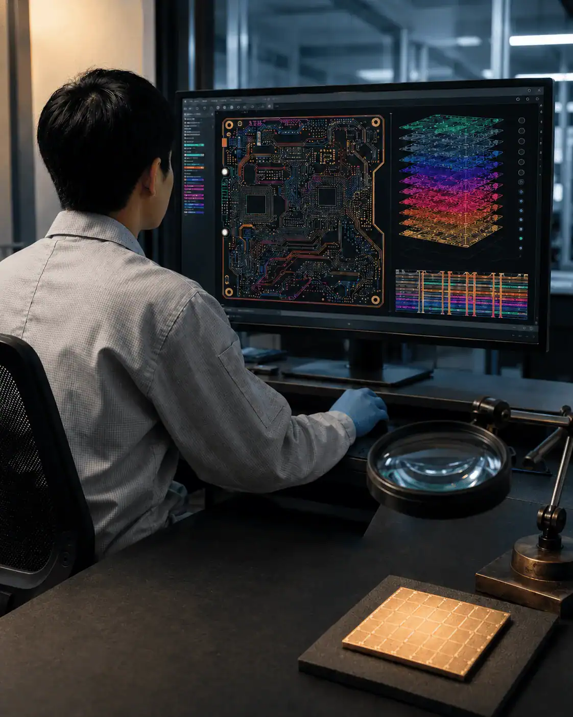
10-Point BT Substrate DFM Checklist
Every point below is audited before tooling — with written notes returned to you for approval.
Package Pitch & Pad Design
BGA / CSP pad diameter, pitch and solder-mask defined vs. non-solder-mask defined pads reviewed against your target package.
Via-in-Pad & Stacked Microvia
Fill quality, capping requirements and stack-up alignment checked for reliable stacked-via structures.
Minimum Line Width & Space
Trace geometry cross-checked against our process capability — flagging critical areas that need mSAP.
Copper Distribution Balance
Per-layer copper density audited for warpage risk — dummy copper suggested where distribution is skewed.
Ultra-Thin Panel Warpage Risk
Board-thickness and layer-symmetry assessed against warpage tolerance for downstream assembly.
Solder Mask Openings & Pad Height
Mask expansion, minimum web and pad-height uniformity confirmed for wire-bond and flip-chip attach.
Surface Finish for Bonding
Wire-bond vs. flip-chip attach requirements matched to ENIG, ENEPIG, soft gold or hard gold.
Panelization & Tooling Holes
Array layout, break-away tabs and fiducials optimized for downstream pick-and-place lines.
Material Thickness & Total Board Thickness
Every layer thickness verified against total-board-thickness target within ±10% tolerance.
Reliability & Acceptance Criteria
IPC-6012 Class 2 or 3 acceptance criteria confirmed with you before production release.
Send us your Gerber and we'll return a written DFM feedback within 24 hours.
No commitment required — audit the report and decide whether to move forward.
Send Your Gerber for a BT PCB Feasibility ReviewQuality Control for BT PCB and IC Substrate Production
Every panel passes 10 inspection stages from incoming material to final shipment — with documented evidence at each step so you can audit the lot before approving delivery.
BT Material & Copper Foil IQC
Every incoming lot verified against manufacturer CoC and internal specs — including Tg, Dk, CTE and copper foil thickness.
Inner-Layer AOI
Automated optical inspection scans every inner layer for opens, shorts and pattern integrity before lamination.
Line Width & Space Measurement
Trace geometry sampled on every panel — verifying fine-line dimensions stay within your IPC Class tolerance.
Layer-to-Layer Registration Check
X-ray verifies inner-layer alignment on complex stack-ups — catching registration drift before drilling.
Microvia & Through-Hole Copper Check
Copper thickness in laser microvias and plated through-holes measured on production coupons.
Microsection Analysis
Cross-section coupons from every lot analyzed for via wall, plating uniformity and layer thickness.
Surface Finish Thickness Test
ENEPIG or ENIG plating thickness measured against your specified layer thickness targets.
100% Electrical Test
Flying-probe test on every panel — no electrical defect makes it past this gate to your assembly line.
Dimensional, Thickness & Warpage QC
Panel dimensions, total board thickness and warpage measured against IPC-6012 acceptance criteria.
Final Visual & Packaging Check
Final cosmetic AOI plus vacuum-sealed moisture-barrier packaging with lot ID labeling.
Every Order Ships With Full Documentation Package
Inspection Report
Panel-level QC results with pass/fail records.
CoC (Certificate of Conformance)
Statement of compliance with your PO spec.
Material Lot Record
BT laminate batch traceability to mill.
Microsection Photo
Cross-section imagery from production coupons.
Electrical Test Record
100% flying-probe test result per panel.
Final Inspection Summary
Consolidated outgoing QC sign-off.
Want sample QC reports from a similar project before you commit?
Request Sample QC PackageWhy Choose QueenEMS as Your BT PCB Manufacturer
A 10-point supplier checklist — the same questions procurement teams use during vendor audits. Every answer backed by real production, real equipment and real certification, not marketing claims.
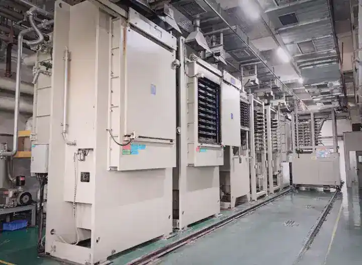
10,000 m² PCB manufacturing plant in Shenzhen
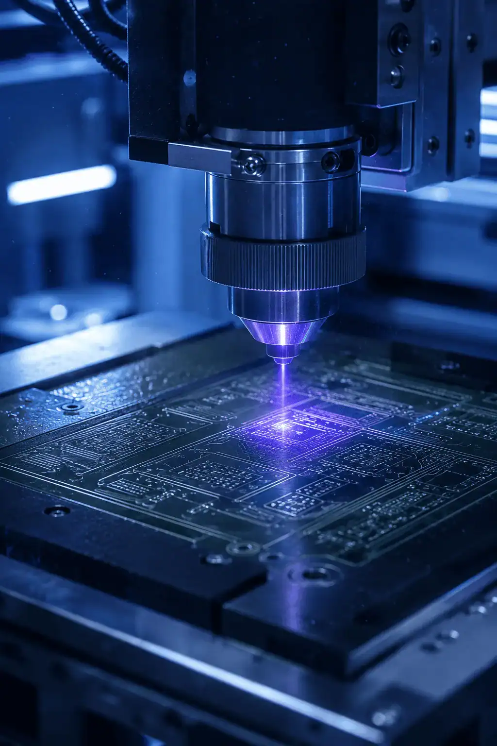

10-Point Supplier Audit — Answered Upfront
The questions procurement teams ask on every vendor audit. Get the answers before you request a quote.
Direct PCB manufacturing support — no middleman broker relaying orders to another factory. You talk directly to the people running the line.
100+ production machines — including LDI imaging, laser drilling, vacuum lamination, plating, AOI and flying-probe test.
High-difficulty PCB process experience — 10+ years shipping HDI, ceramic, RF, heavy-copper and now BT substrate builds.
Engineering-backed communication — substrate engineers join every quote, DFM review and change request.
Quotation within 2 hours during business hours — with engineering feedback on manufacturability, not just a price.
Production and shipping tracking shared via WhatsApp, email or your PM system — no more silence between PO and delivery.
Prototype-to-volume support — one factory scales from 1 panel through 20,000 panels/month without switching suppliers.
Export experience in Europe and North America — regular DHL / FedEx shipments to the US, Canada, Israel and Mexico with export docs handled.
Urgent production support — fast-track lots on qualified stack-ups when your schedule needs to compress.
Clear certification and inspection documentation — ISO 9001, UL, RoHS certificates on request; audited inspection reports on every lot.
Ready to add QueenEMS to your qualified BT PCB vendor list?
Start a Supplier Qualification DiscussionBT substrate is one of 12 board types in our PCB manufacturing services.
BT PCB Manufacturing FAQ
The questions procurement and engineering teams ask most often about BT substrate sourcing. Click any question to see the answer.
What files are required for a BT PCB quotation?
To generate an accurate quote we typically need:
- Gerber files (RS-274X) or ODB++
- Drill file (Excellon format)
- Proposed stack-up with material specification
- Target package type and outline dimensions
- Minimum line width and space
- Surface finish requirement (ENIG, ENEPIG, soft gold, etc.)
- Quantity for prototype and target production volume
Missing information? Send what you have — our substrate engineer will follow up on the specific gaps rather than delay the quote.
What is the difference between BT PCB and standard FR-4 PCB?
The key differences that drive substrate selection:
- CTE: BT resin typically 3–8 ppm/°C X-Y axis vs. FR-4's 14–17 ppm/°C — silicon-die matched for flip-chip reliability.
- Tg: BT commonly ≥185°C (up to 220°C) vs. standard FR-4 at 130–170°C — surviving multiple lead-free reflow cycles.
- Line density: BT substrates support 25/25μm line/space via mSAP; standard FR-4 is typically 75/75μm or 100/100μm.
- Dimensional stability: Lower shrinkage during cure keeps fine-pattern registration on target.
Trade-off: BT substrate cost is meaningfully higher than FR-4 — worth it when your package pitch, thermal budget or reliability target rules FR-4 out.
Can you manufacture ultra-thin BT PCBs?
Yes — our thin-core BT CCL inventory covers 60–200μm cores, and total board thickness down to 0.10 mm is achievable on qualified stack-ups. For ultra-thin builds we run additional warpage inspection and use dedicated handling fixtures through lamination and plating.
Send us the target total thickness and we'll confirm the specific stack-up that meets both your electrical and mechanical requirements.
What surface finish is suitable for wire bonding?
Wire bonding preferences depend on wire type:
- Gold wire bonding: ENEPIG (Ni/Pd/Au) or soft gold — Pd layer improves bond reliability and shelf life.
- Aluminum wire bonding: ENIG works; ENEPIG preferred for higher pull-strength consistency.
- Copper wire bonding: ENEPIG strongly recommended for stable bond formation.
We can adjust gold thickness (typically 0.05–0.15μm for ENEPIG) to match your wire-bond pull-strength spec — send the acceptance criteria and we'll confirm the finish parameters.
How do you control BT PCB warpage?
Warpage control is a stack-up-level discipline, not a single process:
- Low-CTE laminate selection matched to expected thermal profile
- Symmetric copper distribution across all layers (dummy copper added where needed)
- Balanced prepreg and core arrangement in the stack-up
- Controlled lamination pressure and temperature ramp
- Post-lamination bake to relieve residual stress
- Warpage measurement on every panel against IPC-6012 acceptance criteria (≤0.75% typical, ≤0.50% for tight builds)
Can you support BT PCB prototypes before mass production?
Yes — prototypes from 1 panel with fast-track scheduling on qualified stack-ups. Typical prototype turnaround is 10–14 working days for standard BT builds; advanced fine-line or thin-core designs may need 15–20 days.
The prototype run uses the same BT material, same equipment and same process parameters as your production build — so what you validate in the prototype is what you get in mass production.
What information is required for BGA or CSP substrate projects?
Beyond standard PCB files, BGA/CSP projects need:
- Package outline drawing with pitch, ball count and body dimensions
- Die attach method (wire bond or flip chip)
- Bond finger dimensions and pitch (for wire bond)
- Bump pitch and pad diameter (for flip chip)
- Underfill compatibility requirement
- MSL (Moisture Sensitivity Level) target
- Reliability test targets (thermal cycling, HAST, drop test if applicable)
Can you provide material certificates and inspection reports?
Yes — full documentation package ships with every order at no extra cost, including:
- Certificate of Conformance (CoC)
- Material lot record with mill traceability
- Panel-level inspection report
- Microsection photos from production coupons
- 100% electrical test records
- Final outgoing QC summary
Additional documentation (RoHS, REACH, halogen-free reports, IPC-6012 test coupons) available on request.
How long does BT PCB fabrication take?
Typical lead times from confirmed order:
- Prototype (1–5 panels): 10–14 working days
- Standard production (2–8 layer): 15–20 working days
- Complex build-up (10+ layer, 1+4+1 or higher): 20–28 working days
- Ultra-fine line or thin-core builds: +3–5 days
Fast-track scheduling is available on qualified stack-ups when project timing needs to compress — confirmed on a per-order basis.
Can you maintain the same material and process for repeat orders?
Yes — this is a core operating principle for BT substrate customers. Once your first article is approved, we lock:
- BT laminate brand, model and thickness
- Prepreg system and copper foil type
- Stack-up sequence and lamination parameters
- Drilling and plating recipes
- Surface finish process and thickness
- Acceptance criteria and inspection method
Any change to the locked BOM or process — even a laminate lot from a different mill batch — requires written customer approval before we release the order.
Have a question we didn't cover? Our substrate engineers reply within business hours.
Ask a Substrate EngineerGet a BT PCB Feasibility Review Before You Place the Order
Upload what you have — our substrate engineer returns a written feasibility report and a quotation together. No commitment until you approve the DFM feedback.
What to Prepare for the Review
The more items you provide, the tighter the feasibility feedback. Missing something? Send what you have — we'll follow up on the gaps.