
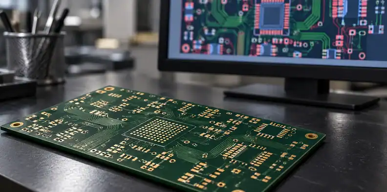
Quick Answer: Send an IPC-D-356 netlist with your Gerber package when you want a separate CAD connectivity reference for the fabricator's data comparison. Export both from the same released design. If the comparison finds a mismatch, resolve its cause and record engineering approval before fabrication; neither file should automatically overrule the other.
A late layout change can leave individually readable files describing different boards. Checking the Gerbers against a netlist extracted from those same Gerbers can repeat the original error. An independent reference gives the review another starting point, provided its source and revision are known.
Do you need an IPC-D-356 netlist with your Gerber files?
An IPC-D-356 netlist is useful when the order requires a check between CAD connectivity and fabrication geometry. It supplements the copper images and drill data with information about nets and their connection points. Gerber and drill files alone can build the board, so agree on format and comparison scope rather than assuming an attached file orders the check.
The format can describe net names, connection locations, pad or pin references, and associated drill information. A fabricator can use that information when comparing manufacturing data and preparing electrical testing. Altium's format overview describes these uses and the distinction between separate netlist files and integrated manufacturing packages.
Gerber files also vary in how much information they carry. Modern attributes can identify connections by net name, as the official Gerber description explains. Ask what your exported package contains and what the receiving CAM workflow will actually compare. A file extension alone does not settle either question.
What does a Gerber-to-netlist comparison actually compare?
The comparison checks connectivity represented by two data inputs. CAM software derives connections from the imported copper and drill geometry, then compares that result with the supplied CAD netlist. Differences can be located by net, reference, side and coordinates. The result describes agreement between those inputs under the selected import and comparison settings.

The import setup is part of the evidence. Layer order, layer assignments and the drill ranges between layers affect how the software reconstructs connections. For a blind-via design, a drill file assigned to the wrong layer range can produce a discrepancy even when the exported geometry is correct.
The documented comparison procedure separates importing the CAD reference, extracting connections from fabrication data and comparing the results. Keep those stages identifiable in the supplier's response. Physical testing happens later; specify its method, coverage and shipment evidence through the separate PCB electrical-test requirements.
Which file should control when the two inputs disagree?
Neither file controls automatically; the authorized engineer decides, after confirming that both inputs represent the same release. A CAD-generated netlist provides a separate reference to check a Gerber export, but an old or incorrectly generated netlist can mislead the review. Establish the source release before deciding which file needs correction or which exception is intentional.
Suppose the layout changed after an earlier netlist export. Sending the new Gerbers alongside that old netlist creates a version dispute before anyone can diagnose a copper problem. Exporting a coherent replacement package resolves the identity question and gives the comparison a meaningful baseline.
Keep the reference's origin visible. A file generated from the released PCB CAD database and one reconstructed from delivered Gerber geometry have different roles. Producing both inputs from the same potentially incorrect geometry removes the independent reference that the check was meant to provide. Even a clean comparison between two outputs of one release shows only that they agree; it cannot show that the released design itself is correct. Net-name attributes help identify connections, while their usefulness still depends on the exported data and receiving workflow.
What should accompany the files sent for comparison?
Provide the complete copper and drill package, the CAD-generated netlist, and an identifier tying both to the same release. Include the layer sequence and applicable drill spans so the fabricator can interpret the geometry. Describe deliberate connections or exceptions by location, with enough detail for engineering to distinguish them from unexplained differences.
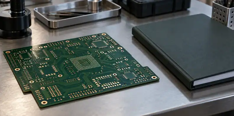
An intentional net tie, for example, needs a defined feature and connection to review. A general note saying that some nets may be shorted leaves the fabricator guessing which reported differences are acceptable. Identify the affected reference or feature, nets and location, then keep the approved explanation with the release.
The requested IPC-D-356 variant should also be explicit. A CAD exporter offering IPC-D-356A and a supplier asking for another accepted input need a format agreement before the package is treated as ready. Confirm how the comparison will be documented and who receives unresolved questions.
Send your Gerber package and BOM for a quotation and free DFM check, adding the netlist and open comparison questions. For a bare-board request, identify that scope; the BOM is relevant when assembly is included.
How should you classify each reported mismatch?
Classify the reported difference as a working diagnosis, then collect evidence before closing it. Start with file identity and import setup, followed by naming, extraction completeness and the actual connection in question. A report category or a large exception count cannot tell you, by itself, whether the design or the fabrication geometry needs changing.
Use this editorial worksheet when reviewing the supplier's difference report:
| Initial finding | Evidence to request | Action before release |
|---|---|---|
| Files represent different releases, or alignment is uncertain | File identities, export source, origin and layer/drill assignments | Restore a coherent input set and repeat the comparison |
| Net names differ at an apparently matching connection | Located nodes and the proposed name mapping | Verify the connection before accepting a naming-only disposition |
| The extracted result omits a connection or object | Source geometry, extraction settings and the specific tool's documented behavior | Investigate the omission; keep the item open until explained |
| A connection is present in one input and absent in the other | Marked location, affected nets and released CAD view | Have engineering correct the data or approve the intentional exception |
The rows organize the investigation; they do not certify the cause. A suspected naming problem can conceal a topology difference, so approving a name mapping requires checking the associated connection.
Altium's comparison procedure for its own CAM editor notes that single-node and no-net objects often appear as missing nets, and that extraction can be incomplete where nested split planes are used. Use that explanation to investigate the reported locations. The same document treats other missing nets as likely extraction problems, so a blanket instruction to ignore all missing nets would close entries nobody has explained, whatever their cause.
Who should approve a mismatch disposition?
Assign the technical disposition to the person authorized to release the design. The fabricator can explain its import settings, correct a setup error and show the resulting comparison. Choosing intended connectivity, accepting a deliberate exception or replacing the released files requires an engineering decision with an identifiable approver and a defined scope.

For a setup correction, retain the corrected interpretation and the repeated comparison. For a design-output error, regenerate the affected package from the accepted source release. For an intentional connection, identify the exact exception and its engineering approval. These outcomes leave different records even if each eventually permits fabrication.
Purchasing should preserve that decision in the order record. An email reply saying “build to Gerber” is too broad if several differences remain unexplained. State which report items the approval covers and which file package the fabricator may use. If an item remains open, keep the affected release on hold rather than extending another item's approval to it.
What should the release record show before fabrication starts?
The release record should connect the accepted CAD release, delivered files, comparison result and engineering dispositions. It should identify what changed when an exception was resolved and point to the final comparison. Keep the approved package retrievable so the fabricator and buyer can establish the exact data authorized for this order.
Use a short record with references to the actual files and report, rather than copying every CAM screen into an email:
| Record field | What to retain |
|---|---|
| Design baseline | Part number, revision and accepted CAD release identifier |
| Input package | Exact Gerber, drill and netlist filenames, with export date or file checksums |
| Comparison basis | Reference provenance, layer/drill interpretation and relevant settings |
| Exception register | Report item, net, reference or feature, side and location |
| Disposition | Cause, correction or approved exception, responsible engineer and date |
| Final authorization | Final package identity, repeated comparison where needed, and approval to fabricate |
Both worksheets are purchasing recommendations built around the documented comparison workflow, not IPC forms or measured test results.
QueenEMS has more than 10 years of experience and offers flying probe, ICT and functional testing; those physical tests follow the data comparison and do not replace it. The applicable checks still belong in the quotation and order scope. Use the PCB capabilities page for the manufacturing discussion, and confirm the proposed input format and comparison arrangement before committing the release.
What else should you confirm about netlist checks?
Confirm where the reference came from, whether the receiving workflow uses embedded net information, how unresolved report items are handled and what physical testing follows fabrication. Keeping these questions separate helps you request the right evidence. An accepted file package, a closed comparison report and a finished-board test result represent different decisions in the order.
Should the IPC-D-356 netlist be generated from the Gerber files?
No, if its purpose is an independent reference for checking those Gerbers. Export it from the accepted CAD release. A netlist reconstructed from the Gerber geometry is the other comparison input and can reproduce an error already present in that geometry.
Do ODB++ or IPC-2581 packages need a separate IPC-D-356 file?
Not always. Those formats can include connectivity within the manufacturing package. Confirm that the receiving workflow accepts the package and uses that information for the agreed check before omitting a separately requested file.
Can missing nets in the report be ignored?
No blanket waiver is appropriate. Check the affected objects, locations and extraction behavior. Document why each accepted exception is harmless or provide corrected data and repeat the comparison.
Does a clean comparison mean the boards passed electrical test?
No. The comparison evaluates manufacturing data before physical boards are tested. Obtain the separately agreed production-test evidence for the fabricated lot.
Send your Gerber files and BOM to request pricing and a free DFM review. Include the matching netlist, release identifier and any located discrepancies; state whether the request covers bare boards or assembly.
Upload your files today · Free DFM check before production · Ship worldwide
Get your PCB prototypes in as fast as 24 hours. We handle FR4, Rogers, and hybrid boards, with standard builds up to 24 layers and higher layer counts subject to engineering review — free prototypes for 2–4 layer FR-4 boards, no minimum order.
Just upload your Gerber + BOM — we source every part, assemble, and inspect (AOI + X‑Ray) so you don't have to chase suppliers. PCB assembly typically takes 5–8 working days once all components are in stock. The confirmed delivery schedule is subject to your quotation.